Overview of the Gerber File Format
The Gerber file format was originally developed by the Gerber Systems Corp. in the 1960s for their vector photoplotters. It has since become the de facto standard for PCB fabrication data exchange. Gerber files are ASCII text files that use a series of commands to describe the geometric features on each layer of the PCB.
The current version of the Gerber format is referred to as Extended Gerber or X2. It includes enhancements over the older Standard Gerber format (RS-274-D) such as embedded aperture definitions and attributes. However, both formats are still widely used and supported.
Anatomy of a Gerber File
A Gerber file consists of the following main sections:
- Header: Contains information like file name, creation date, format version etc.
- Aperture definitions: Defines the shapes and sizes of the “drawing tools”.
- Data blocks: The actual vector coordinates and drawing commands.
- M02: End-of-file indicator.
Here’s a simple example of Gerber data:
%FSLAX24Y24*%
%MOIN*%
%ADD10C,0.010*%
D10*
X0100Y0100D02*
X0500Y0100D01*
X0500Y0500D01*
X0100Y0500D01*
X0100Y0100D01*
M02*
Layers in a PCB Gerber File Package
A complete Gerber PCB fabrication package consists of multiple files, one for each layer of the board. The common layers are:
| Layer | File Extension | Description |
|---|---|---|
| Top Copper | .GTL | Top layer copper traces |
| Bottom Copper | .GBL | Bottom layer copper traces |
| Top Soldermask | .GTS | Top solder resist mask |
| Bottom Soldermask | .GBS | Bottom solder resist mask |
| Top Silkscreen | .GTO | Top overlay legend |
| Bottom Silkscreen | .GBO | Bottom overlay legend |
| Drill Files | .DRL, .TXT | NC drill hole information |
| Board Outline | .GM1 | PCB profile routing paths |
The file extensions are not standardized, but the Gerber X2 format allows embedding the layer type within the file as attributes.
PCB Fabrication Process Using Gerber Files
The typical PCB manufacturing process using Gerber files involves the following steps:
1. Design and Output
The PCB designer creates the schematic and board layout using EDA (Electronic Design Automation) tools like Altium, Eagle, KiCad etc. After design verification, the Gerber files are generated from the EDA tool.
2. Gerber File Check and Optimization
The fabricator imports the Gerber files into their CAM (Computer-Aided Manufacturing) software to perform design rule checks (DRC). Common checks include:
- Minimum trace width and spacing
- Minimum drill hole size
- Copper-to-edge clearance
- Solder mask clearance
If issues are found, the designer is notified to make corrections. The fabricator may also optimize the data, for example by collapsing duplicate pads.
3. Film Plotting and Printing
The optimized Gerber data is used to plot the photographic film or directly expose the photoresist on the copper-clad laminates. Each layer has its own film.
4. Etching and Plating
The exposed laminates undergo a series of chemical baths to etch away the unwanted copper, leaving only the desired circuit pattern. If the design has plated through-holes (PTH), they are drilled and electroplated at this stage.
5. Solder Mask and Silkscreen
A solder mask lacquer is applied and exposed using the solder mask films. This insulates the copper traces. The silkscreen legend is then printed on the solder mask.
6. Surface Finish
The exposed pads are plated with the specified surface finish, such as HASL (Hot Air Solder Leveling), ENIG (Electroless Nickel Immersion Gold), or OSP (Organic Solderability Preservative).
7. Profiling and Routing
The PCB panel is routed or punched out into individual boards based on the outline Gerber data.
8. Electrical Test and Inspection
The fabricated PCBs undergo automated optical inspection (AOI) and electrical continuity test to check for manufacturing defects. A cross-section analysis may also be performed on sample boards for quality control.

Tips for Creating Quality Gerber Files
To avoid manufacturing issues and delays, PCB designers should follow these best practices when generating Gerber files:
- Use the latest Extended Gerber (X2) format if possible for added intelligence.
- Ensure all files are included and named correctly.
- Include reference designators for easier communication.
- Adhere to the fabricator’s design guidelines and constraints.
- Specify requirements like material type, thickness, color, and surface finish.
- Generate NC drill files in Excellon format with embedded tool sizes.
- Provide a ReadMe file detailing the PCB specs, layer structure, and instructions.
- Review the generated Gerber data in a viewer before sending out.
Frequently Asked Questions (FAQ)
1. What is the difference between Standard Gerber (RS-274D) and Extended Gerber (RS-274X)?
Standard Gerber, also known as RS-274D, is the legacy Gerber format. It has limitations like lack of standardized aperture definitions and layer types. Extended Gerber or RS-274X introduced enhancements such as embedded aperture definitions and file attributes. It allows for more intelligent and unambiguous data interpretation.
2. Can I use other formats besides Gerber for PCB fabrication?
While Gerber is the most widely used PCB data transfer format, some fabricators may accept other formats such as ODB++ (Open Database++), IPC-2581, or even native CAD files. However, Gerber remains the safest and most universal choice for compatibility.
3. What is the typical resolution of Gerber files?
Gerber files use integer coordinates. The resolution is specified by the coordinate format, such as 2.3 or 2.4, where the integer part indicates the number of digits before the decimal point, and the fractional part is the number of digits after. For example, 2.4 format has a resolution of 0.1 mil (0.0001 inch). The choice of resolution depends on the minimum feature size of the PCB design.
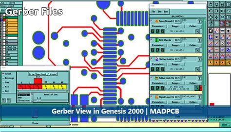
4. How do I check my Gerber files before sending them out for fabrication?
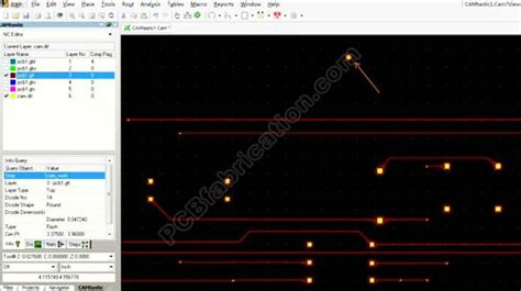
It’s important to review your generated Gerber files in a Gerber viewer software before submitting them for manufacturing. Many free and paid Gerber viewers are available, such as GC-Prevue, ViewMate, and Ucamco UcamX. These viewers allow you to layer by layer and check for any errors or discrepancies.
5. What should I do if my PCB fabricator reports issues with my Gerber files?
If your PCB manufacturer informs you of problems with your Gerber data, such as missing layers, incorrect formatting, or design rule violations, you should regenerate the files after making the necessary corrections in your PCB design software. It’s also a good idea to communicate with your fabricator and clarify their requirements and guidelines to avoid delays.
Conclusion
The Gerber file format is the backbone of the PCB fabrication industry. By understanding the Gerber file structure, layer types, and the manufacturing process, PCB designers can create reliable and high-quality Gerber data for successful PCB fabrication. Following best practices and working closely with the fabricator can help ensure a smooth and error-free manufacturing experience.
No responses yet