Introduction to Fanout PCB
In the world of printed circuit board (PCB) design, optimizing the use of available space is crucial for creating compact, efficient, and cost-effective electronic devices. One key strategy for maximizing PCB real estate is the implementation of fanout techniques. Fanout PCB design involves the strategic placement and routing of components and traces to ensure optimal connectivity while minimizing the overall footprint of the board.
This article will delve into the various fanout strategies employed by PCB designers to make the most of limited board space. We will explore the benefits of fanout PCB design, discuss different approaches to component placement and routing, and provide practical examples of how these techniques can be applied in real-world scenarios.
The Importance of Efficient PCB Real Estate Utilization
Miniaturization Trends in Electronics
The electronics industry has been witnessing a consistent trend towards miniaturization. Consumers demand smaller, more portable devices with increased functionality, putting pressure on PCB designers to create compact and efficient layouts. By utilizing fanout strategies, designers can accommodate more components and features within a limited space, enabling the development of smaller and more advanced electronic products.
Cost Reduction through Optimized PCB Design
Efficient utilization of PCB real estate not only contributes to miniaturization but also helps reduce manufacturing costs. By minimizing the overall footprint of the board, designers can reduce the amount of raw materials required, such as the substrate, copper, and solder mask. Additionally, optimized layouts can simplify the manufacturing process, reducing the likelihood of errors and improving yields, further contributing to cost savings.
Improved Signal Integrity and Performance
Fanout PCB design plays a crucial role in maintaining signal integrity and overall system performance. By carefully placing components and routing traces, designers can minimize signal interference, crosstalk, and other adverse effects that can degrade the quality of the electrical signals. Proper fanout techniques ensure that signals travel efficiently from one component to another, reducing signal losses and improving the overall reliability of the electronic device.
Fanout Techniques for Component Placement
Ball Grid Array (BGA) Fanout
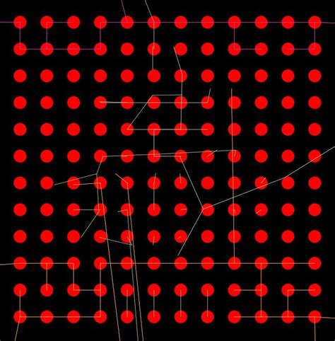
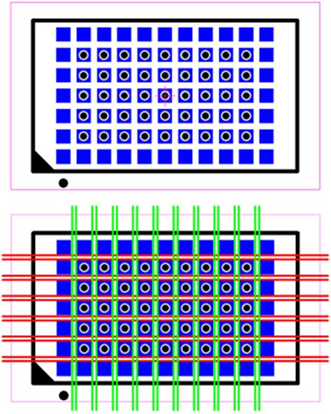
Ball Grid Array (BGA) packages are widely used in modern electronics due to their high pin count and compact size. However, routing traces from the densely packed BGA pads to other components on the PCB can be challenging. BGA fanout techniques involve strategically placing and routing traces to ensure proper connectivity while minimizing the impact on surrounding components.
One common BGA fanout approach is the “dog bone” technique, where short traces are used to connect the BGA pads to via pads located slightly outward from the package. This allows for a more organized and efficient routing of traces to other parts of the board. Another technique is the use of micro vias, which are small diameter vias that can be placed directly on the BGA pads, enabling a higher density of connections.
Quad Flat Pack (QFP) Fanout
Quad Flat Pack (QFP) packages are another popular choice for PCB designers due to their relatively high pin count and moderate size. QFP fanout involves the placement and routing of traces from the package leads to other components on the board. To optimize space utilization, designers often employ a technique called “via fanout,” where vias are placed near the QFP leads to route traces to the inner layers of the PCB.
By using via fanout, designers can reduce the number of traces on the outer layers, freeing up space for other components and routing. Additionally, via fanout helps in reducing signal interference and crosstalk by allowing for a more organized and separated routing of traces.
Discrete Component Fanout
Discrete components, such as resistors, capacitors, and inductors, are essential building blocks in electronic circuits. Efficient placement and routing of these components can significantly impact the overall PCB layout. One fanout strategy for discrete components is to place them in a staggered pattern, allowing for a more compact arrangement and easier routing of traces.
Another approach is to use surface-mount devices (SMDs) with smaller footprints, such as 0201 or 01005 packages, which occupy less space on the board. By carefully selecting the appropriate package sizes and arranging them in a space-efficient manner, designers can maximize the available PCB real estate.

Routing Strategies for Fanout PCB Design
Via Placement and Optimization
Vias are essential elements in PCB design, allowing for the interconnection of traces between different layers of the board. However, vias also consume valuable PCB real estate, making their placement and optimization crucial for efficient fanout design. One strategy is to use blind and buried vias, which are vias that do not extend through the entire thickness of the board. By using blind and buried vias, designers can create more direct connections between layers, reducing the need for long traces and saving space on the outer layers.
Another approach is to use via-in-pad techniques, where vias are placed directly on the component pads. This eliminates the need for additional via pads and allows for a more compact routing of traces. However, via-in-pad design requires careful consideration of manufacturability and reliability aspects.
Trace Width and Spacing Optimization
The width and spacing of traces play a significant role in PCB real estate utilization. By optimizing trace widths based on the required current carrying capacity and signal integrity requirements, designers can minimize the space occupied by traces. Additionally, by using appropriate spacing between traces, designers can reduce crosstalk and signal interference while maintaining a compact layout.
High-speed signals may require wider traces and greater spacing to maintain signal integrity, while low-speed signals can be routed with narrower traces and tighter spacing. By carefully balancing these requirements and using appropriate design rules, designers can achieve an efficient and reliable fanout PCB layout.
Multi-Layer PCB Design
Utilizing multiple layers in a PCB is another effective strategy for maximizing real estate. By distributing components and traces across different layers, designers can create a more compact and organized layout. Inner layers can be used for power and ground planes, providing a low-impedance path for power distribution and reducing the need for dedicated power traces on the outer layers.
Signal layers can be strategically placed to minimize the length of traces and reduce signal interference. By using a combination of blind, buried, and through vias, designers can create efficient interconnections between layers, enabling a more optimized fanout design.
Practical Examples of Fanout PCB Design
Example 1: Smartphone PCB Layout
Smartphone PCBs are prime examples of the need for efficient fanout design. With the increasing demand for more features and functionality in a compact form factor, smartphone PCB designers must utilize every available space on the board. By using BGA fanout techniques, such as dog bone and micro via placement, designers can accommodate high-density components like processors and memory modules.
QFP fanout techniques, such as via fanout, enable efficient routing of traces from the peripheral components to the inner layers of the board. Discrete components can be placed in a staggered pattern and routed using optimized trace widths and spacing to minimize the overall footprint.
Example 2: Internet of Things (IoT) Device PCB Layout
IoT devices often require a balance between functionality and size, making fanout PCB design crucial for their success. These devices typically incorporate sensors, wireless communication modules, and power management components, all of which must be efficiently placed and routed on the board.
By using multi-layer PCB design, designers can separate the power and ground planes from the signal layers, reducing noise and interference. BGA and QFP fanout techniques can be employed to route traces from the high-density components to other parts of the board. Discrete components can be selected in smaller package sizes and placed strategically to maximize space utilization.
Example 3: Automotive Electronic Control Unit (ECU) PCB Layout
Automotive ECUs require robust and reliable PCB designs that can withstand harsh environmental conditions. Fanout techniques play a critical role in ensuring the proper functioning and longevity of these devices. By using via fanout and optimized trace widths, designers can create a more robust and reliable interconnection between components.
Multi-layer PCB design can be employed to separate sensitive signals from noisy power lines, improving signal integrity and reducing electromagnetic interference (EMI). BGA and QFP fanout techniques can be used to route traces from the high-density components to other parts of the board, while discrete components can be placed and routed in a space-efficient manner.
Fanout PCB Design Considerations and Best Practices
Design Rule Checking (DRC)
Design Rule Checking (DRC) is a crucial step in the PCB design process, ensuring that the layout adheres to the specified design rules and constraints. When implementing fanout techniques, it is essential to perform thorough DRC to identify and resolve any violations or conflicts. This includes checking for minimum trace widths, spacing, via sizes, and other parameters specific to the manufacturing process and the desired performance of the board.
By running DRC regularly during the fanout design process, designers can catch and rectify issues early, avoiding costly redesigns and manufacturing delays.
Collaboration with PCB Manufacturers
Collaborating closely with PCB manufacturers is essential for successful fanout PCB design. Manufacturers have specific capabilities, limitations, and preferences based on their equipment and processes. By engaging with the manufacturer early in the design phase, designers can ensure that their fanout strategies are compatible with the manufacturing process and can be efficiently produced.
Manufacturers can provide valuable input on design rules, material selection, and other factors that influence the manufacturability and reliability of the fanout PCB. By incorporating this feedback into the design, designers can optimize the layout for manufacturing and avoid potential issues during production.
Simulation and Verification
Simulation and verification are critical steps in validating the performance and reliability of fanout PCB designs. By using electronic design automation (EDA) tools, designers can simulate the behavior of the circuit, analyze signal integrity, and identify potential issues before committing to physical prototypes.
Signal integrity simulations can help designers optimize trace widths, spacing, and terminations to ensure proper signal propagation and minimize reflections and crosstalk. Thermal simulations can assess the heat dissipation and thermal management aspects of the fanout design, ensuring that components operate within their specified temperature ranges.
By conducting thorough simulations and verifications, designers can refine their fanout strategies, optimize performance, and reduce the risk of design failures.
Frequently Asked Questions (FAQ)
1. What is fanout in PCB design?
Fanout in PCB design refers to the technique of strategically placing and routing components and traces to ensure optimal connectivity while minimizing the overall footprint of the board. It involves the efficient utilization of available PCB real estate to accommodate more components and features within a limited space.
2. Why is fanout important in PCB design?
Fanout is important in PCB design because it enables the creation of compact, efficient, and cost-effective electronic devices. By maximizing the utilization of PCB real estate, designers can accommodate more components and features in a smaller form factor, reduce manufacturing costs, and improve signal integrity and overall system performance.
3. What are some common fanout techniques for component placement?
Some common fanout techniques for component placement include:
– Ball Grid Array (BGA) fanout: Using techniques like dog bone and micro via placement to route traces from densely packed BGA pads to other components on the board.
– Quad Flat Pack (QFP) fanout: Employing via fanout techniques to route traces from QFP leads to inner layers of the PCB, reducing trace congestion on outer layers.
– Discrete component fanout: Placing components in a staggered pattern and using smaller package sizes to maximize space utilization.
4. How does multi-layer PCB design help in fanout?
Multi-layer PCB design helps in fanout by allowing designers to distribute components and traces across different layers, creating a more compact and organized layout. Inner layers can be used for power and ground planes, reducing the need for dedicated power traces on outer layers. Signal layers can be strategically placed to minimize trace lengths and reduce signal interference.
5. What are some best practices for successful fanout PCB design?
Some best practices for successful fanout PCB design include:
– Conducting thorough Design Rule Checking (DRC) to ensure the layout adheres to specified design rules and constraints.
– Collaborating closely with PCB manufacturers to ensure fanout strategies are compatible with their capabilities and processes.
– Performing simulations and verifications to validate the performance and reliability of fanout designs before committing to physical prototypes.
– Optimizing trace widths, spacing, and terminations to ensure proper signal integrity and minimize signal degradation.
– Utilizing appropriate via placement and optimization techniques to create efficient interconnections between layers.
Conclusion
Fanout PCB design is a crucial aspect of creating compact, efficient, and reliable electronic devices. By utilizing various fanout strategies for component placement and routing, designers can maximize the available PCB real estate, accommodate more features and functionality, and improve overall system performance.
This article has explored the importance of efficient PCB real estate utilization, discussed different fanout techniques for component placement and routing, and provided practical examples of how these strategies can be applied in real-world scenarios. We have also highlighted important considerations and best practices for successful fanout PCB design, including Design Rule Checking, collaboration with manufacturers, and simulation and verification.
As the demand for smaller and more advanced electronic devices continues to grow, the importance of fanout PCB design will only increase. By staying up-to-date with the latest fanout techniques and best practices, PCB designers can create innovative and efficient layouts that meet the evolving needs of the electronics industry.
Efficient utilization of PCB real estate through fanout design is not only a technical challenge but also an opportunity for innovation and advancement in the field of electronics. By pushing the boundaries of what is possible with limited space, designers can unlock new possibilities and create products that shape the future of technology.
No responses yet