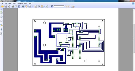
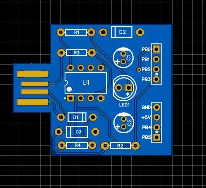
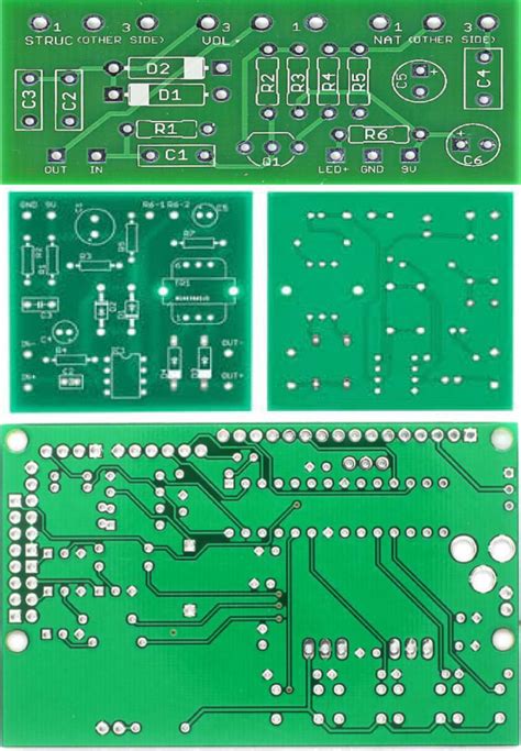
Introduction to PCB Templates
Printed Circuit Board (PCB) design is a complex process that requires careful planning, attention to detail, and adherence to industry standards. To streamline the design process and ensure consistency across projects, many engineers and designers rely on PCB templates. These templates provide a starting point for new designs, incorporating best practices, common components, and layout guidelines.
In this article, we will explore the benefits of using PCB templates in design development, discuss key considerations when creating or selecting templates, and provide examples of how templates can be used effectively in various applications.
Benefits of Using PCB Templates
Improved Efficiency
One of the primary benefits of using PCB templates is improved efficiency in the design process. By starting with a pre-designed template, engineers can save time and effort that would otherwise be spent on creating basic layouts, placing common components, and setting up design rules. This allows them to focus on the unique aspects of their design, such as component selection and placement, routing, and optimization.
Consistency and Standardization
PCB templates promote consistency and standardization across projects. By establishing a set of common design elements, such as layer stackups, component footprints, and naming conventions, templates ensure that all designs within an organization follow the same guidelines. This consistency makes it easier for team members to collaborate, review designs, and troubleshoot issues.
Reduced Errors and Rework
Using PCB templates can help reduce errors and the need for rework in the design process. Templates incorporate best practices and design rules that have been proven to work in previous projects, minimizing the risk of common mistakes. By starting with a well-tested template, designers can avoid issues related to component placement, signal integrity, and manufacturability, ultimately saving time and resources.
Creating Effective PCB Templates
Identify Common Design Elements
To create an effective PCB template, start by identifying the common design elements that are used across multiple projects. These elements may include:
- Layer stackups
- Board sizes and shapes
- Component footprints
- Power and ground planes
- Connector locations
- Mounting holes
By incorporating these common elements into a template, designers can ensure that they are consistently applied to all projects.
Define Design Rules and Constraints
PCB templates should include a set of design rules and constraints that govern the placement and routing of components. These rules may include:
- Minimum trace widths and spacings
- Via sizes and drill pairs
- Clearance and creepage distances
- Differential pair routing guidelines
- High-speed signal routing constraints
By defining these rules upfront, designers can ensure that their layouts meet industry standards and are optimized for manufacturability.
Use Hierarchical Design Techniques
Hierarchical design techniques can be used to create modular, reusable PCB templates. By breaking down a design into smaller, self-contained blocks, designers can create templates for common circuit functions, such as power supplies, amplifiers, and interface circuits. These blocks can then be combined to form larger, more complex designs.
Using hierarchical design techniques can also make it easier to update and maintain templates over time. If a particular block needs to be modified or optimized, it can be updated independently of the rest of the design.
Incorporate Best Practices and Industry Standards
PCB templates should incorporate best practices and industry standards to ensure that designs are reliable, manufacturable, and compliant with relevant regulations. Some key considerations include:
- Component placement guidelines
- Thermal management
- Electromagnetic compatibility (EMC)
- Electrostatic discharge (ESD) protection
- Design for manufacturing (DFM) principles
By incorporating these best practices into templates, designers can ensure that their designs meet the highest standards of quality and performance.

Using PCB Templates in Practice
Selecting the Right Template
When starting a new PCB design project, it’s important to select the right template for the job. Consider the following factors when choosing a template:
- Board size and shape
- Layer count and stackup
- Component types and footprints
- Signal integrity requirements
- Power supply and distribution needs
By selecting a template that closely matches the requirements of the project, designers can minimize the amount of customization needed and accelerate the design process.
Customizing Templates for Specific Applications
While PCB templates provide a solid foundation for new designs, they may need to be customized to meet the specific requirements of a particular application. This may involve adding or removing components, adjusting layout parameters, or modifying design rules.
When customizing a template, it’s important to document any changes made and the rationale behind them. This documentation can be used to help other team members understand the design decisions and can serve as a reference for future projects.
Iterating and Optimizing Designs
PCB templates provide a starting point for new designs, but they are not a substitute for the iterative process of optimization and refinement. As designers work with a template, they may identify areas for improvement, such as component placement, routing, or signal integrity.
By using simulation tools and analysis techniques, designers can optimize their designs for performance, reliability, and manufacturability. This iterative process of design, analysis, and refinement is critical to creating high-quality PCBs that meet the needs of the application.
PCB Template Examples
To illustrate the use of PCB templates in practice, let’s consider a few examples:
Example 1: Power Supply Template
A power supply template might include the following elements:
- AC/DC converter
- Voltage regulators
- Filtering capacitors
- Protection circuitry
- Connector footprints
By creating a standardized power supply template, designers can ensure that all power supplies within an organization follow the same basic architecture and meet the same performance and safety requirements.
Example 2: High-Speed Digital Interface Template
A high-speed digital interface template might include the following elements:
- Differential pair routing
- Impedance-controlled traces
- Termination resistors
- Decoupling capacitors
- Connector footprints
By using a standardized template for high-speed digital interfaces, designers can ensure that their designs meet signal integrity requirements and are optimized for reliable data transfer.
Example 3: Analog Sensor Interface Template
An analog sensor interface template might include the following elements:
- Amplifier circuitry
- Analog-to-digital converter (ADC)
- Filtering components
- Connector footprints
By using a standardized template for analog sensor interfaces, designers can ensure that their designs are optimized for signal fidelity and can be easily integrated with other system components.
Frequently Asked Questions (FAQ)
-
Q: What are the benefits of using PCB templates in design development?
A: Using PCB templates can improve efficiency, promote consistency and standardization across projects, and reduce errors and the need for rework in the design process. -
Q: How do I create an effective PCB template?
A: To create an effective PCB template, identify common design elements, define design rules and constraints, use hierarchical design techniques, and incorporate best practices and industry standards. -
Q: What factors should I consider when selecting a PCB template for a new project?
A: When selecting a PCB template, consider factors such as board size and shape, layer count and stackup, component types and footprints, signal integrity requirements, and power supply and distribution needs. -
Q: Can PCB templates be customized for specific applications?
A: Yes, PCB templates can be customized to meet the specific requirements of a particular application. This may involve adding or removing components, adjusting layout parameters, or modifying design rules. -
Q: How can I optimize my PCB design using a template?
A: To optimize your PCB design using a template, use simulation tools and analysis techniques to identify areas for improvement, such as component placement, routing, or signal integrity. Engage in an iterative process of design, analysis, and refinement to create a high-quality PCB that meets the needs of the application.
Conclusion
PCB templates are a valuable tool for engineers and designers looking to streamline the design process, ensure consistency across projects, and reduce errors and rework. By creating effective templates that incorporate best practices, common design elements, and industry standards, organizations can accelerate the development of high-quality PCBs that meet the needs of a wide range of applications.
When using PCB templates, it’s important to select the right template for the job, customize it as needed for specific applications, and engage in an iterative process of optimization and refinement. By following these guidelines and leveraging the benefits of templates, designers can create PCBs that are reliable, manufacturable, and optimized for performance.
| PCB Template Type | Key Elements | Benefits |
|---|---|---|
| Power Supply | – AC/DC converter – Voltage regulators – Filtering capacitors – Protection circuitry – Connector footprints |
– Standardized architecture – Consistent performance and safety requirements |
| High-Speed Digital Interface | – Differential pair routing – Impedance-controlled traces – Termination resistors – Decoupling capacitors – Connector footprints |
– Optimized signal integrity – Reliable data transfer |
| Analog Sensor Interface | – Amplifier circuitry – Analog-to-digital converter (ADC) – Filtering components – Connector footprints |
– Optimized signal fidelity – Easy integration with other system components |
By leveraging the power of PCB templates and following best practices in design development, engineers and designers can create high-quality, reliable PCBs that meet the needs of a wide range of applications. As the complexity of electronic systems continues to grow, the use of templates will become increasingly important in accelerating innovation and ensuring the success of PCB design projects.
No responses yet