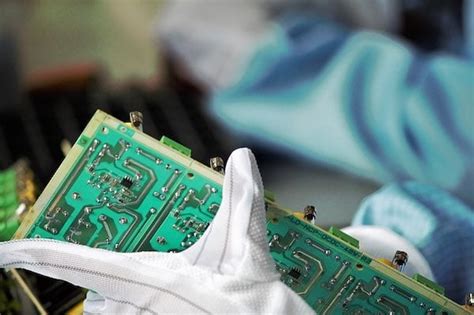
Introduction to PCB Troubleshooting
Printed Circuit Board (PCB) design is a complex process that involves multiple steps, from schematic design to board layout and manufacturing. Despite the best efforts of designers and engineers, issues can arise at any stage of the process, leading to problems with the final product. PCB troubleshooting is the process of identifying and resolving these issues to ensure that the board functions as intended.
In this article, we will explore the various aspects of PCB troubleshooting, including common issues, diagnostic techniques, and best practices for avoiding problems in the first place.
Common PCB Issues
There are several common issues that can arise during the PCB design and manufacturing process. These include:
Short Circuits
Short circuits occur when two or more conductive paths on the PCB are unintentionally connected, causing current to flow in an unintended direction. This can be caused by a variety of factors, including:
- Incorrect component placement
- Solder bridges between traces
- Damaged or broken traces
- Conductive debris on the board
Open Circuits
Open circuits occur when a conductive path on the PCB is broken or interrupted, preventing current from flowing. This can be caused by:
- Broken or damaged traces
- Incorrectly soldered components
- Missing or damaged components
Component Failure
Component failure can occur due to a variety of reasons, including:
- Incorrect component selection
- Overheating or thermal stress
- Electrical overload or surge
- Manufacturing defects
Signal Integrity Issues
Signal integrity issues can arise when the electrical signals on the PCB are distorted or degraded, leading to incorrect or unreliable operation. This can be caused by:
- Impedance mismatches
- Crosstalk between traces
- Reflections and ringing
- Electromagnetic interference (EMI)
PCB Troubleshooting Techniques
When issues arise with a PCB, there are several techniques that can be used to diagnose and resolve the problem. These include:
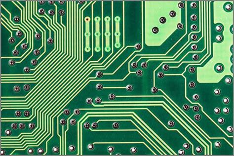
Visual Inspection
Visual inspection is the first step in PCB troubleshooting. This involves carefully examining the board for any obvious signs of damage or defects, such as:
- Broken or damaged components
- Solder bridges or shorts
- Incorrect component placement
- Damaged or broken traces
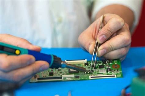
Continuity Testing
Continuity testing is used to verify that the conductive paths on the PCB are intact and connected as intended. This can be done using a multimeter or continuity tester to measure the resistance between two points on the board.
Voltage and Current Measurements
Voltage and current measurements can be used to verify that the board is receiving the correct power supply and that the components are operating within their specified ranges. This can be done using a multimeter or oscilloscope to measure the voltage and current at various points on the board.
Thermal Imaging
Thermal imaging can be used to identify areas of the board that are overheating or experiencing thermal stress. This can be done using a thermal camera or infrared thermometer to measure the temperature at various points on the board.
Signal Analysis
Signal analysis involves measuring and analyzing the electrical signals on the PCB to identify any issues with signal integrity or timing. This can be done using an oscilloscope or logic analyzer to capture and analyze the waveforms on the board.

Best Practices for PCB Design and Manufacturing
While PCB troubleshooting is an important skill, the best way to avoid issues is to follow best practices for PCB design and manufacturing from the start. Some key best practices include:
Careful Component Selection
Choosing the right components for the application is critical to ensuring reliable operation and avoiding issues such as overheating or electrical overload. When selecting components, consider factors such as:
- Voltage and current ratings
- Temperature ratings
- Package size and type
- Availability and cost
Proper Grounding and Shielding
Proper grounding and shielding are essential for minimizing issues with signal integrity and EMI. This includes:
- Using a solid ground plane on the PCB
- Properly routing power and ground traces
- Using shielding techniques such as ground planes and guard traces
- Minimizing the loop area of high-frequency signals
Thorough Testing and Validation
Thorough testing and validation are essential for identifying and resolving issues before the board goes into production. This includes:
- Design rule checking (DRC) to verify that the board meets manufacturing and assembly requirements
- Electrical rule checking (ERC) to verify that the schematic is correct and free of errors
- Prototype testing to verify that the board functions as intended
- Environmental testing to ensure that the board can withstand the expected operating conditions
Collaboration and Communication
Effective collaboration and communication between the design team, manufacturing team, and other stakeholders are essential for avoiding issues and ensuring a successful project. This includes:
- Clearly defining requirements and specifications
- Regularly reviewing and discussing design progress
- Identifying and addressing potential issues early in the process
- Maintaining clear and accurate documentation throughout the project
Frequently Asked Questions (FAQ)
Q1: What are the most common causes of PCB failure?
A1: The most common causes of PCB failure include short circuits, open circuits, component failure, and signal integrity issues. These can be caused by a variety of factors, including incorrect component selection, manufacturing defects, thermal stress, and electrical overload.
Q2: How can I prevent short circuits on my PCB?
A2: To prevent short circuits on your PCB, follow best practices such as careful component placement, proper trace routing, and thorough cleaning to remove any conductive debris. Additionally, use techniques such as solder masks and conformal coatings to protect against accidental shorts.
Q3: What tools do I need for PCB troubleshooting?
A3: The basic tools needed for PCB troubleshooting include a multimeter, oscilloscope, logic analyzer, and thermal camera or infrared thermometer. Additional tools such as a microscope and soldering iron may also be useful depending on the specific issue.
Q4: How can I improve signal integrity on my PCB?
A4: To improve signal integrity on your PCB, follow best practices such as proper grounding and shielding, minimizing trace lengths and loop areas, and using appropriate termination techniques. Additionally, consider using simulation tools to analyze and optimize the signal paths on the board.
Q5: What should I do if I suspect a component failure on my PCB?
A5: If you suspect a component failure on your PCB, first perform a visual inspection to look for any obvious signs of damage or defects. Next, use a multimeter to measure the voltage and current at the component pins to verify that it is receiving the correct power supply. If the component still appears to be faulty, it may need to be replaced.
Conclusion
PCB troubleshooting is an essential skill for anyone involved in the design and manufacturing of electronic products. By understanding the common issues that can arise and the techniques used to diagnose and resolve them, you can ensure that your PCBs are reliable, high-quality, and meet the needs of your application.
However, the best approach to PCB troubleshooting is to avoid issues in the first place by following best practices for design and manufacturing. By carefully selecting components, properly grounding and shielding the board, thoroughly testing and validating the design, and maintaining effective collaboration and communication throughout the project, you can minimize the risk of issues and ensure a successful outcome.
No responses yet