Using Autorouting for Everything
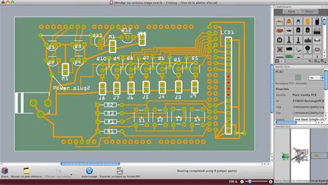
One piece of misguided advice is to rely entirely on autorouting tools to route all the traces on your PCB. While autorouting can be a useful aid, it should not be relied upon exclusively. Autorouting algorithms don’t always produce the most efficient or reliable routing, especially for complex high-speed or analog circuits.
Issues with blind autorouting include:
- Inefficient use of board space
- Traces routed too close together causing crosstalk
- Improper impedance control
- Lack of length matching for differential pairs
- No consideration for EMI
The bottom line is autorouting is no substitute for careful manual routing, at least for the most critical traces. Use autorouting to save time on simpler, less critical connections, but route important signals by hand.
Ignoring Manufacturability
Another terrible PCB design tip is to focus purely on electrical functionality while ignoring manufacturing considerations. Just because a board passes DRC in your CAD tool doesn’t mean it can actually be produced!
Problems that can arise from manufacturing ignorant designs include:
| Issue | Cause | Impact |
|---|---|---|
| Acid traps | Acute angles in copper | Etching issues |
| Tombstoning | Uneven pad sizes | Components misalign during reflow |
| Starved thermals | Insufficient heat transfer | Soldering problems |
| Impossibly small features | Violating fab limits | Board can’t be made |
To avoid these pitfalls, always consult with your manufacturer and follow their published DFM guidelines for aspects like:
- Minimum trace width and spacing
- Pad sizes and shapes
- Drill sizes and annular rings
- Soldermask requirements
Adhering to DFM rules from the start prevents delays and additional costs later. Your manufacturer is your partner, not your adversary.

Skimping on Vias
Via abuse is another common PCB design anti-pattern. Vias are essential for routing multilayer boards but should be used judiciously. Using too few vias causes issues like:
- Excessive detours to route around obstacles
- Longer traces leading to increased resistance and inductance
- Ground bounce and other noise problems on high-speed signals
However, via overuse is problematic too, causing:
- Increased board cost
- Manufacturing problems if vias are too small
- Wasted board real estate
- Potential EMI antennas from poorly implemented vias
The key is balance – use enough vias for efficient routing and solid grounding but not superfluously. And ensure your vias are properly designed:
- Size them appropriately for manufacturing
- Provide sufficient annular ring
- Stitch or stagger longer vias to improve reliability
- Avoid vias under BGA pads

Forgetting the Ground Plane
Trying to save on layer count by skipping a proper ground plane is a major mistake. A solid ground plane is essential for signal integrity, power delivery, noise control, and EMI reduction.
Misconceptions like “I don’t need a ground plane since I’m only doing low-speed digital” are flat-out wrong. Even if EMI isn’t a concern, a ground plane keeps return paths short, provides shielding between layers, and helps with power distribution.
Multi-point grounding with a patchwork of copper fills is not an adequate substitute. This can actually cause more problems than it solves due to unintended slots becoming radiating antennas.
At a minimum, every PCB should have at least one continuous ground plane covering the entire board. Two is even better – a power plane and a ground plane forming a parallel plate capacitor. For the best results on 6+ layer boards:
| Layer | Function |
|---|---|
| Top | Signals + components |
| L2 | Ground |
| L3 | Power |
| L4 | Signals |
| L5 | Power |
| L6 | Ground |
| Bottom | Signals + components |

Improper Decoupling
Proper supply decoupling with capacitors is critical for power integrity. But there’s a lot of misinformation out there about how to do it right.
Some common bad advice includes:
- “Decoupling caps are optional if the power supply is good” (Wrong! Caps are still needed to handle transient current demands)
- “Place decoupling caps anywhere they’ll fit” (No – they need to be as close to IC power pins as possible)
- “Bulk caps on the power input are sufficient” (Local high-frequency caps are also essential)
- “Any cap value will do” (Different frequencies require different capacitor values)
In reality, effective decoupling requires:
- Bulk capacitance (1uF+) on the board power input to absorb low frequency noise
- Local mid-frequency caps (0.1-1uF) near IC power pins to handle transients
- High frequency caps (0.01uF or less) as close as possible to VCC/GND pins
- Low ESR/ESL caps for best high frequency performance
- Multiple caps in parallel to reduce overall ESR
Not Backannotating
One often neglected step is back-annotating your PCB Routing into your schematic. Not doing this is a recipe for confusion later.
Back-annotation accomplishes two important things:
- Updates the schematic with actual routed net names which may differ from your original names
- Allows you to compare original schematic connectivity to actual PCB connections to verify nothing was missed
Without backannotation, there’s no guarantee that the schematic matches the physical board. Weeks or months later when you have to debug an issue or do a revision, mismatches between schematic and layout waste time and invite errors.
Make backannotation part of your standard design process. All professional CAD tools support this. There’s no excuse not to do it.
Failing to Plan
Perhaps the most fundamental bad PCB advice is not making a plan before starting design. Proper planning prevents poor performance! Without a solid plan, you’re inviting all kinds of issues down the road.
Key planning steps include:
- Defining a complete block diagram and BOM
- Selecting an appropriate physical form factor
- Determining the number of layers needed
- Choosing a stack-up based on impedance and EMC needs
- Identifying critical components and signals
- Establishing placement and routing priorities
- Setting DFM rules and manufacturability targets
- Agreeing voltage/power domains and decoupling strategy
Trying to figure this all out on the fly is hugely inefficient. Making a plan doesn’t have to take long but it will save massive amounts of time and headaches later. Measure twice, cut once!
FAQ
What’s the single most important thing to get right in PCB layout?
Proper grounding. Get your grounding scheme right with a continuous ground plane and you’ll eliminate many potential signal integrity and EMI problems before they start. Grounding is the foundation that everything else is built on.
Is it okay to route power traces on a signal layer?
For low-power designs, sure. But for anything more than a few hundred milliamps, power traces should be on dedicated layers. Trying to route power on signal layers leads to issues like ground bounce, crosstalk, and voltage drop. It’s also much harder to manage power flow when mixed with signals.
Do I really need to worry about controlled impedance?
It depends on your signaling speeds. For designs under ~50 MHz, impedance control is usually not necessary. But above that or for sensitive analog circuits, controlled impedance routing is essential for reliable operation. When in doubt, consult your manufacturer – they can advise if your design requires impedance control.
What’s an acceptable amount of crosstalk between traces?
The answer depends on your circuit’s noise margin and the magnitude of your signals. As a general rule, you want crosstalk to be at least 40-50 dB down from your signal level. For a 3.3V digital signal, that equates to less than ~30mV of induced noise. The wider the trace spacing and the farther apart routing layers are, the less crosstalk will occur.
How small can I make my vias?
That depends on your PCB manufacturer’s capabilities. Most fabs have a lower limit around 0.2-0.3mm drill size. Any smaller than that and you’ll pay a premium, if it’s even possible. Also consider that smaller vias are harder to manufacture reliably and can cause soldering issues. Stick to your vendor’s published DFM guidelines and when in doubt, go bigger, not smaller.
In conclusion, there’s a lot of bad PCB design advice floating around. Blindly following unsound practices can lead to all sorts of expensive and time-consuming issues. Always think critically, consult experts, and trust data over unsubstantiated opinions. With the proper approach, you’ll be well on your way to creating successful, reliable PCB designs that meet your requirements. Happy routing!

No responses yet