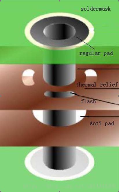
What is Thermal Relief?
Thermal relief is a crucial aspect of printed circuit board (PCB) design that helps to prevent thermal stress and damage to components during the soldering process. In PCB manufacturing, components are subjected to high temperatures during reflow soldering, which can cause thermal expansion and contraction. This thermal stress can lead to cracking, delamination, and other forms of damage to the PCB and its components. Thermal relief design involves creating specific patterns and features in the PCB layout to minimize thermal stress and ensure reliable solder connections.
Importance of Thermal Relief in PCB Design
Incorporating thermal relief in PCB design offers several benefits:
- Reduced thermal stress on components
- Improved solder joint reliability
- Enhanced PCB durability and longevity
- Minimized risk of component damage during soldering
- Better heat dissipation and thermal management
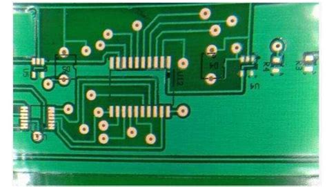
Thermal Relief Patterns
There are several common thermal relief patterns used in PCB design, each with its own advantages and considerations.
Spoke Pattern
The spoke pattern is one of the most widely used thermal relief designs. It consists of four or more thin traces, called spokes, that connect the pad to the surrounding copper pour. The spokes allow heat to dissipate quickly during soldering while maintaining a reliable electrical connection.
Advantages:
– Easy to implement in PCB design software
– Provides good thermal relief and heat dissipation
– Suitable for most component types
Considerations:
– Spoke width and length need to be optimized for specific components and PCB requirements
– May require additional space around the component pad
Teardrop Pattern
The teardrop pattern is similar to the spoke pattern but features teardrop-shaped openings at the end of each spoke. This design helps to reduce stress concentrations and improve the mechanical strength of the solder joint.
Advantages:
– Enhances mechanical strength of the solder joint
– Reduces stress concentrations at the spoke-pad interface
– Provides good thermal relief and heat dissipation
Considerations:
– Requires more complex PCB design compared to the spoke pattern
– May not be suitable for high-density layouts with limited space
C-Shaped Pattern
The C-shaped pattern consists of a circular or semicircular opening around the component pad, with a small connecting trace. This design allows for efficient heat dissipation while maintaining a compact footprint.
Advantages:
– Compact design suitable for high-density layouts
– Provides good thermal relief and heat dissipation
– Easy to implement in PCB design software
Considerations:
– May not provide as much mechanical strength as other patterns
– Connecting trace width needs to be optimized for specific components and PCB requirements
Thermal Relief Pattern Comparison
| Pattern | Thermal Relief | Mechanical Strength | Layout Complexity |
|---|---|---|---|
| Spoke | Good | Moderate | Low |
| Teardrop | Good | High | Moderate |
| C-Shaped | Good | Moderate | Low |
Thermal Relief Design Considerations
When implementing thermal relief in PCB design, several factors need to be considered to ensure optimal performance and reliability.
Component Type and Size
Different components have varying thermal mass and heat dissipation requirements. Larger components, such as power inductors and transformers, may require more substantial thermal relief designs compared to smaller components like resistors and capacitors. It is essential to consider the specific component requirements when selecting and optimizing thermal relief patterns.
PCB Material and Thickness
The choice of PCB material and thickness can impact the effectiveness of thermal relief designs. Thicker PCBs and those made from materials with higher thermal conductivity, such as aluminum-backed PCBs, may require different thermal relief approaches compared to standard FR-4 PCBs. It is important to consider the thermal properties of the PCB material when designing thermal relief patterns.
Solder Mask and Paste Coverage
Solder mask and paste coverage can affect the thermal relief design’s performance. Adequate solder mask clearance around the thermal relief pattern is necessary to ensure proper solder flow and prevent bridging. Similarly, the solder paste coverage should be optimized to provide sufficient solder volume for a reliable joint without causing excessive solder buildup or spillage.
Copper Pour and Trace Width
The width of the copper pour surrounding the thermal relief pattern and the width of the connecting traces play a crucial role in heat dissipation and mechanical strength. Wider copper pours and traces can provide better thermal conductivity and mechanical stability, but they may also increase the overall PCB size and manufacturing cost. It is essential to strike a balance between thermal performance, mechanical strength, and layout efficiency when designing thermal relief patterns.

Thermal Relief Optimization Techniques
To optimize thermal relief designs for specific PCB requirements, several techniques can be employed.
Simulation and Modeling
Using thermal simulation and modeling tools can help to predict the thermal behavior of the PCB and its components during the soldering process. These tools can provide valuable insights into the effectiveness of different thermal relief patterns and help to identify potential issues before manufacturing.
Design Rule Checks (DRC)
Incorporating thermal relief design rules into the PCB design software’s DRC can help to ensure that the thermal relief patterns meet the required specifications. DRC rules can check for minimum spoke width, solder mask clearance, and other critical parameters to prevent design errors and ensure manufacturability.
Experimental Validation
Conducting experimental validation of thermal relief designs can provide real-world data on the effectiveness of different patterns and optimization techniques. This can involve thermal imaging, cross-sectioning, and mechanical testing of solder joints to assess the thermal relief design’s performance and reliability.
Frequently Asked Questions (FAQ)
-
What is the purpose of thermal relief in PCB design?
Thermal relief in PCB design helps to minimize thermal stress and damage to components during the soldering process by providing a path for heat dissipation and reducing thermal expansion and contraction. -
What are the most common thermal relief patterns?
The most common thermal relief patterns are the spoke pattern, teardrop pattern, and C-shaped pattern. Each pattern has its own advantages and considerations in terms of thermal relief, mechanical strength, and layout complexity. -
How does PCB material and thickness affect thermal relief design?
The choice of PCB material and thickness can impact the effectiveness of thermal relief designs. Thicker PCBs and those made from materials with higher thermal conductivity may require different thermal relief approaches compared to standard PCBs. -
What role does solder mask and paste coverage play in thermal relief design?
Solder mask and paste coverage can affect the performance of the thermal relief design. Adequate solder mask clearance around the thermal relief pattern is necessary to ensure proper solder flow, while optimized solder paste coverage provides sufficient solder volume for a reliable joint. -
How can thermal relief designs be optimized for specific PCB requirements?
Thermal relief designs can be optimized using techniques such as simulation and modeling, design rule checks (DRC), and experimental validation. These methods help to predict thermal behavior, ensure design integrity, and validate the effectiveness of different optimization approaches.
Conclusion
Thermal relief design is a critical aspect of PCB design that ensures reliable solder connections and minimizes the risk of component damage during the soldering process. By understanding the different thermal relief patterns, design considerations, and optimization techniques, PCB designers can create robust and efficient layouts that meet the specific requirements of their applications. Properly implemented thermal relief designs contribute to improved PCB durability, enhanced thermal management, and overall system reliability.
No responses yet