What is Rogers PCB and Why Use It?
Rogers PCB refers to printed circuit boards made from Rogers Corporation’s high frequency laminate materials. These specialty materials offer superior electrical properties compared to standard FR-4, making Rogers PCBs ideal for high-speed digital, RF/microwave, and advanced driver assistance applications that demand optimal signal integrity and reliability.
Key advantages of Rogers PCB include:
– Low dielectric loss for minimal signal attenuation
– Consistent dielectric constant over a wide frequency range
– Excellent thermal conductivity for heat dissipation
– Dimensional stability at high temperatures
– Smooth, uniform surface for precise trace geometries
To maximize these benefits and ensure peak performance, consider the following 8 technical tips when designing your Rogers PCB.
1. Select the Right Rogers Material
Rogers offers a portfolio of PCB laminates to meet various design requirements. Each material has unique characteristics in terms of dielectric constant (Dk), dissipation factor, thermal conductivity, and thickness.
Some popular Rogers materials include:
| Material | Dk @ 10 GHz | Dissipation Factor @ 10 GHz | Thermal Conductivity (W/m/K) | Thickness (mm) |
|---|---|---|---|---|
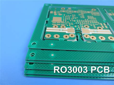
| RO3003 | 3.00 | 0.0010 | 0.50 | 0.127 – 1.524 |
| RO4350B | 3.48 | 0.0037 | 0.62 | 0.168 – 1.524 |
| RO4835 | 3.32 | 0.0030 | 0.69 | 0.101 – 1.016 |
| RT/duroid 6006 | 6.15 | 0.0019 | 0.44 | 0.127 – 2.997 |
Consider your application’s frequency, bandwidth, insertion loss, and thermal requirements to select a suitable dielectric. Generally, lower Dk correlates with higher signal speeds, while lower loss tangent (dissipation factor) means less signal attenuation.
2. Optimize Trace Dimensions
Trace width and thickness directly impact impedance, propagation delay, and current carrying capacity. Thinner traces yield higher characteristic impedance but also increase DC resistance. Work with your manufacturer to establish minimum trace widths and copper weights for your selected Rogers material and desired impedance.
To calculate trace dimensions for a target impedance, use the following formulas:
Microstrip
Characteristic Impedance (Zo):
Zo = 87 / √(εr + 1.41) * ln(5.98 * h / (0.8 * w + t))
Stripline
Characteristic Impedance (Zo):
Zo = 60 / √εr * ln(4 * h / (0.67 * π * (0.8 * w + t)))
Where:
– εr = dielectric constant
– h = dielectric thickness (mm)
– w = trace width (mm)
– t = trace thickness (mm)
Online calculators and your EDA tool’s field solver can also assist with impedance calculations and trace sizing.

3. Minimize Discontinuities
Discontinuities along a trace, such as vias, bends, and transitions between layers, can cause reflections and degrade signal quality. While impossible to eliminate completely, you can minimize their impact through careful design:
- Route differential pairs on the same layer with length matching
- Avoid 90° corners in traces; use 45° bends or arcs instead
- Perform via stitching and backdrilling to reduce stub resonance
- Maintain constant trace width and spacing through turns
- Gradually taper trace width when transitioning between layers
If a via is unavoidable, use a smaller drill size to reduce parasitics. Microvias with 0.1-0.15 mm diameter are often used in high speed designs.
4. Maintain Proper Grounding
A solid ground plane is crucial for signal integrity and EMI suppression in Rogers PCB designs. It provides a low impedance return path for currents and shields against crosstalk.
Some grounding best practices include:
- Use uninterrupted ground planes on outer layers
- Stitch ground planes together with vias where necessary
- Avoid split ground planes if possible
- Connect ground pours on signal layers to main ground with ample vias
- Surround sensitive traces with via fences tied to ground
For mixed signal boards, implement separate analog and digital ground planes joined at a single point to prevent noise coupling.
5. Employ Shielding Techniques
Copper shielding can further bolster noise immunity and prevent radiation leakage from the PCB. You can implement shielding in several ways:
- Placing copper pours around sensitive traces and components
- Sandwiching signal layers between ground planes
- Designing the board with an enclosed Faraday cage
- Specifying a metallic shield can for the entire assembly
In all cases, ensure the shield is properly grounded with multiple vias along its perimeter. Aim for via spacing of λ/10 – λ/20 at the highest frequency of concern.
6. Optimize Power Delivery
Stable power distribution is essential to reduce noise and maintain signal integrity. Key considerations include:
- Place decoupling capacitors close to ICs, with short traces to power and ground
- Use wide traces and copper pours for power rails to minimize IR drop
- Isolate analog and digital power supplies to prevent crosstalk
- Specify appropriate voltage regulator modules for each supply rail
When designing the stackup, use dedicated power planes instead of traces where possible. Thicker dielectrics between power and ground planes may be necessary to support higher voltage rails.
7. Simulate and Verify the Design
Before manufacturing, simulate your Rogers PCB design to validate signal integrity and identify potential issues. Some important analyses include:
- Time Domain Reflectometry (TDR) to assess impedance and discontinuities
- Electromagnetic Interference (EMI) simulation to check for radiated emissions
- Thermal simulation to verify heat dissipation and prevent hot spots
- Signal integrity simulation to analyze eye diagrams, jitter, and bit error rate
Many EDA tools offer built-in simulators for these tasks. Alternatively, you can export data to specialized simulation software for more in-depth analysis.
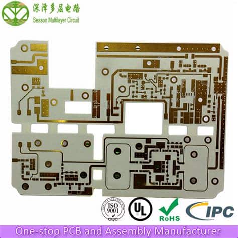
8. Work with an Experienced Manufacturer
Fabricating and assembling Rogers PCBs requires specialized processes and expertise beyond standard FR-4 boards. Look for a manufacturer with ample experience in Rogers material handling, impedance control routing, and advanced HDI techniques.
Key capabilities to look for include:
- Laser drilling for small microvias
- Controlled-depth backdrilling for stub removal
- Automated optical inspection (AOI) for precise measurements
- Flying probe and ICT testing for comprehensive validation
Discuss your design intent and performance requirements with the manufacturer early on. They can provide valuable feedback on manufacturability, reliability, and cost optimization.
FAQ
1. How do I select the right Rogers material for my application?
Consider your design’s frequency, bandwidth, loss tolerance, and thermal requirements. Higher frequencies and wider bandwidths benefit from lower dielectric constant materials like RO3003. For applications sensitive to insertion loss, choose materials with lower dissipation factors such as RO4350B. If thermal management is a concern, look for higher thermal conductivity materials like RO4835.
2. What is the ideal impedance for Rogers PCB traces?
The target impedance depends on your application and signaling standards. Common impedances include:
- 50 Ω for RF/microwave and high speed digital designs
- 75 Ω for video and some telecommunications standards
- 90-110 Ω for differential pairs in high speed digital interfaces
Work with your system designer and refer to relevant standards to determine the appropriate impedance for your design.
3. How can I minimize crosstalk between traces on a Rogers PCB?
To reduce crosstalk, follow these guidelines:
- Route adjacent traces orthogonally to each other
- Increase spacing between parallel traces
- Place ground traces or pours between sensitive signals
- Use tighter coupling for differential pairs to promote common-mode noise rejection
- Avoid routing traces over splits in the ground plane
Performing a 3D electromagnetic simulation can also help identify and mitigate potential crosstalk issues.
4. What is the recommended hole size and pad diameter for vias on Rogers PCBs?
The specific drill size and pad diameter depend on your via type and Rogers material thickness. In general:
- For through-hole vias, use a drill size of 0.2-0.3 mm and a pad diameter of 0.6-0.8 mm
- For microvias, use a drill size of 0.1-0.15 mm and a pad diameter of 0.25-0.35 mm
- For buried/blind vias, consult with your manufacturer for recommended sizes based on the layer stackup
Always confirm the minimum drill size and aspect ratio that your fabricator can reliably manufacture.
5. How do I ensure my Rogers PCB design is manufacturable?
To improve manufacturability and avoid delays, follow these tips:
- Adhere to your manufacturer’s design rules and guidelines for your chosen Rogers material
- Use standard trace and space widths that are compatible with the fabricator’s process capabilities
- Specify copper weights and plating thicknesses that are readily available
- Minimize the number of unique drill sizes and use standard hole diameters where possible
- Allow for adequate manufacturing tolerances on impedance-controlled traces
- Communicate any special requirements or non-standard features to your fabricator early in the design process
By collaborating closely with an experienced Rogers PCB manufacturer, you can ensure a smooth transition from design to production.
No responses yet