Introduction to PCB Documentation
Printed Circuit Board (PCB) assembly documentation is a crucial aspect of the electronics manufacturing process. It ensures that all stakeholders, from designers to manufacturers and assemblers, have access to the necessary information to build a functional and reliable product. Proper PCB documentation helps streamline the assembly process, reduce errors, and facilitate effective communication between teams.
In this article, we will discuss seven essential tips for preparing comprehensive and effective PCB Assembly documentation. By following these guidelines, you can ensure that your documentation is accurate, clear, and easily accessible to all parties involved in the manufacturing process.
Tip 1: Create a Bill of Materials (BOM)
What is a Bill of Materials?
A Bill of Materials (BOM) is a comprehensive list of all the components required to assemble a PCB. It includes details such as part numbers, quantities, descriptions, and supplier information. The BOM serves as a reference for the procurement team and helps ensure that all necessary components are available for the assembly process.
Key Elements of a BOM
A well-structured BOM should include the following information:
- Part Number: A unique identifier for each component
- Description: A brief description of the component
- Quantity: The number of each component required for the assembly
- Manufacturer: The name of the component manufacturer
- Manufacturer Part Number: The manufacturer’s unique identifier for the component
- Supplier: The name of the supplier from whom the component will be purchased
- Supplier Part Number: The supplier’s unique identifier for the component
- Reference Designator: The location of the component on the PCB
Best Practices for Creating a BOM
- Use a consistent format throughout the BOM
- Ensure that all part numbers and descriptions are accurate and up-to-date
- Include alternate part numbers or suppliers, if applicable
- Review and update the BOM regularly to reflect any changes in the design or component availability

Tip 2: Develop a PCB Assembly Drawing
What is a PCB Assembly Drawing?
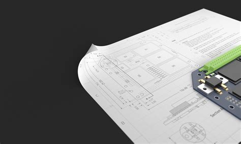
A PCB assembly drawing is a visual representation of the PCB that provides clear instructions for the assembly process. It includes information such as component placement, orientation, and soldering requirements. The assembly drawing helps ensure that the PCB is assembled correctly and consistently, reducing the risk of errors and rework.
Key Elements of a PCB Assembly Drawing
A comprehensive PCB assembly drawing should include the following information:
- Board Outline: The physical dimensions and shape of the PCB
- Component Placement: The location and orientation of each component on the PCB
- Reference Designators: The unique identifiers for each component, corresponding to the BOM
- Polarity Indicators: Markings to indicate the correct orientation of polarized components (e.g., capacitors, diodes)
- Soldering Requirements: Specifications for soldering, such as pad sizes, solder mask openings, and solder paste stencil thickness
- Assembly Notes: Any special instructions or considerations for the assembly process
Best Practices for Creating a PCB Assembly Drawing
- Use clear and consistent symbols and notations
- Ensure that the drawing is legible and easy to understand
- Include detailed views or enlargements for complex areas of the PCB
- Provide a legend or key to explain any symbols or abbreviations used in the drawing

Tip 3: Provide Schematics and Gerber Files
What are Schematics and Gerber Files?
Schematics are graphical representations of the electrical connections and components in a PCB design. They provide a high-level overview of how the components are interconnected and how the circuit functions. Gerber files, on the other hand, are the industry-standard format for describing the physical layout of a PCB. They contain information about the copper layers, solder mask, silkscreen, and drill holes.
Importance of Schematics and Gerber Files in PCB Documentation
Providing schematics and Gerber files as part of the PCB documentation is essential for several reasons:
- They enable the manufacturer to fabricate the PCB accurately
- They allow for design review and verification before production begins
- They serve as a reference for troubleshooting and repairs
- They facilitate communication between the design and manufacturing teams
Best Practices for Providing Schematics and Gerber Files
- Ensure that the schematics and Gerber files are up-to-date and match the final PCB design
- Use a consistent naming convention for the files
- Include a README file that describes the contents and purpose of each file
- Verify that the Gerber files adhere to the manufacturer’s specifications and requirements

Tip 4: Include a PCB Stackup Diagram
What is a PCB Stackup Diagram?
A PCB stackup diagram is a cross-sectional view of the layers in a PCB. It shows the arrangement and thickness of the copper layers, insulating layers (e.g., FR-4), and any additional layers such as solder mask or silkscreen. The stackup diagram helps the manufacturer understand the structure of the PCB and ensures that the board is fabricated correctly.
Key Elements of a PCB Stackup Diagram
A comprehensive PCB stackup diagram should include the following information:
- Layer Arrangement: The order and orientation of the layers in the PCB
- Layer Thicknesses: The thickness of each layer, including copper, insulating material, and any additional layers
- Material Specifications: The type and properties of the materials used in each layer (e.g., copper weight, FR-4 grade)
- Impedance Requirements: Any specific impedance requirements for controlled impedance designs
- Finish Requirements: The type of surface finish to be applied to the PCB (e.g., HASL, ENIG, OSP)
Best Practices for Creating a PCB Stackup Diagram
- Use a clear and concise layout that is easy to understand
- Ensure that the layer thicknesses and materials are accurately specified
- Include any special requirements, such as controlled impedance or specific surface finishes
- Review the stackup diagram with the manufacturer to ensure that it meets their capabilities and requirements
Tip 5: Specify Assembly Instructions
Why are Assembly Instructions Important?
Assembly instructions provide clear and detailed guidance for the PCB assembly process. They help ensure that the components are placed and soldered correctly, and that any special requirements or procedures are followed. Well-written assembly instructions can reduce the risk of errors, improve the efficiency of the assembly process, and ultimately lead to a higher-quality final product.
Key Elements of Assembly Instructions
Comprehensive assembly instructions should include the following information:
- Assembly Sequence: The order in which components should be placed and soldered onto the PCB
- Placement Requirements: Any specific requirements for component placement, such as orientation or spacing
- Soldering Requirements: The type of soldering to be used (e.g., wave, reflow, hand), as well as any specific temperature profiles or solder paste specifications
- Inspection Guidelines: Criteria for visual inspection of the assembled PCB, including acceptable solder joint characteristics and component placement tolerances
- Special Instructions: Any additional steps or procedures required for the assembly process, such as applying conformal coating or programming firmware
Best Practices for Specifying Assembly Instructions
- Use clear and concise language that is easy to understand
- Include visual aids, such as photographs or diagrams, to illustrate key steps or requirements
- Ensure that the instructions are consistent with the information provided in the BOM, assembly drawing, and other documentation
- Review the instructions with the assembly team to ensure that they are comprehensive and practical
Tip 6: Include Testing and Quality Control Procedures
Importance of Testing and Quality Control in PCB Assembly
Testing and quality control procedures are essential for ensuring that the assembled PCBs meet the required performance and reliability standards. These procedures help identify any defects or issues early in the production process, reducing the risk of costly rework or product failures in the field. Effective testing and quality control also help maintain the consistency and quality of the final product.
Key Elements of Testing and Quality Control Procedures
A comprehensive set of testing and quality control procedures should include the following:
- Visual Inspection: Guidelines for visually inspecting the assembled PCBs for defects such as incorrect component placement, solder bridges, or damaged components
- Electrical Testing: Procedures for testing the electrical functionality of the PCB, such as continuity tests, voltage measurements, and functional tests
- Environmental Testing: Requirements for testing the PCB under various environmental conditions, such as temperature, humidity, or vibration, to ensure its reliability and durability
- Acceptance Criteria: Clear definitions of what constitutes a pass or fail for each test or inspection, as well as any required corrective actions for failures
- Documentation: Instructions for documenting the results of each test or inspection, including any issues encountered and corrective actions taken
Best Practices for Including Testing and Quality Control Procedures
- Develop a comprehensive testing plan that covers all aspects of the PCB’s functionality and reliability
- Ensure that the testing and quality control procedures are consistent with industry standards and customer requirements
- Provide clear and detailed instructions for each test or inspection, including setup, execution, and evaluation criteria
- Regularly review and update the procedures based on feedback from the production team and any changes in the product or process
Tip 7: Maintain Clear Revision Control
Importance of Revision Control in PCB Documentation
PCB designs often go through multiple iterations and revisions during the development process. Effective revision control ensures that all stakeholders are working with the most up-to-date and accurate version of the documentation. This helps prevent confusion, errors, and delays in the production process.
Key Elements of Revision Control
A robust revision control system should include the following elements:
- Revision Numbering: A consistent and logical scheme for assigning revision numbers to each version of the documentation
- Change History: A record of the changes made in each revision, including the date, author, and a brief description of the changes
- Document Control: A system for managing and distributing the latest version of the documentation to all relevant stakeholders
- Archiving: A process for archiving older versions of the documentation for reference and traceability
Best Practices for Maintaining Revision Control
- Establish a clear and consistent revision numbering scheme that is easy to understand and follow
- Maintain a detailed change history that captures all significant modifications to the documentation
- Ensure that all stakeholders are working with the latest version of the documentation
- Regularly review and update the documentation to reflect any changes in the design or production process
- Archive older versions of the documentation in a secure and easily accessible location
FAQs
1. What is the difference between a schematic and a Gerber file?
A schematic is a graphical representation of the electrical connections and components in a PCB design, while a Gerber file is a standard format for describing the physical layout of a PCB, including the copper layers, solder mask, and drill holes.
2. Why is it important to include a bill of materials (BOM) in the PCB documentation?
A bill of materials (BOM) is essential because it provides a comprehensive list of all the components required to assemble the PCB. It helps ensure that the procurement team has all the necessary information to purchase the correct components and that the assembly team has a clear reference for the build process.
3. What should be included in a PCB stackup diagram?
A PCB stackup diagram should include the arrangement and thickness of the copper layers, insulating layers, and any additional layers such as solder mask or silkscreen. It should also specify the material properties, impedance requirements, and finish requirements for the PCB.
4. How can clear assembly instructions help improve the quality of the final PCB product?
Clear and detailed assembly instructions help ensure that the components are placed and soldered correctly, and that any special requirements or procedures are followed. This reduces the risk of errors, improves the efficiency of the assembly process, and ultimately leads to a higher-quality final product.
5. Why is revision control important in PCB documentation?
Revision control is important because it ensures that all stakeholders are working with the most up-to-date and accurate version of the documentation. This helps prevent confusion, errors, and delays in the production process, especially when the PCB design undergoes multiple iterations and revisions during development.
Conclusion
Preparing comprehensive and effective PCB assembly documentation is essential for ensuring a smooth and efficient production process. By following the seven tips outlined in this article – creating a bill of materials, developing a PCB assembly drawing, providing schematics and Gerber files, including a PCB stackup diagram, specifying assembly instructions, including testing and quality control procedures, and maintaining clear revision control – you can create documentation that is accurate, clear, and easily accessible to all stakeholders.
Investing time and effort into creating high-quality PCB documentation can help reduce errors, improve communication between teams, and ultimately lead to a higher-quality final product. By adopting these best practices and continually refining your documentation processes, you can streamline your PCB assembly workflow and ensure the success of your electronic products.
No responses yet