Introduction to PCBA Defects
Printed Circuit Board Assembly (PCBA) is a crucial process in the manufacturing of electronic devices. It involves the assembly of various components onto a printed circuit board (PCB) to create a functional electronic circuit. However, during the PCBA process, various defects can occur, which can lead to malfunctions or complete failure of the electronic device. In this article, we will discuss seven common PCBA manufacturing defects and their solutions.
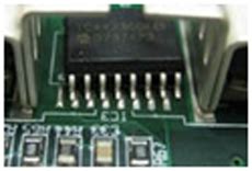
1. Solder Bridges
What are Solder Bridges?
Solder bridges are a common PCBA defect that occurs when excess solder connects two or more adjacent pads or traces on the PCB, creating an unintended electrical connection. This can lead to short circuits, which can cause the electronic device to malfunction or fail.
Causes of Solder Bridges
- Excessive solder paste application
- Improper solder paste stencil design
- Incorrect reflow oven temperature profile
- Inadequate cleaning of the PCB before soldering
- Incorrect component placement
Solutions for Solder Bridges
- Optimize the solder paste stencil design to ensure the correct amount of solder paste is applied
- Adjust the reflow oven temperature profile to ensure proper solder melting and flow
- Clean the PCB thoroughly before soldering to remove any contaminants
- Use automated optical inspection (AOI) systems to detect solder bridges early in the manufacturing process
- Implement proper training and quality control measures for manual soldering processes

2. Cold Solder Joints
What are Cold Solder Joints?
Cold solder joints occur when the solder does not melt completely, resulting in a weak and unreliable connection between the component and the PCB. This can cause intermittent electrical connections, leading to device malfunction or failure.
Causes of Cold Solder Joints
- Insufficient solder paste application
- Incorrect reflow oven temperature profile
- Inadequate preheating of the PCB and components
- Contamination of the PCB or components
- Improper component placement
Solutions for Cold Solder Joints
- Optimize the solder paste stencil design to ensure sufficient solder paste is applied
- Adjust the reflow oven temperature profile to ensure proper solder melting and flow
- Ensure proper preheating of the PCB and components before soldering
- Clean the PCB and components thoroughly before soldering to remove any contaminants
- Use automated optical inspection (AOI) systems to detect cold solder joints early in the manufacturing process

3. Tombstoning
What is Tombstoning?
Tombstoning, also known as chipstanding or drawbridging, is a defect that occurs when a surface-mounted component (SMD) stands up on one end instead of lying flat on the PCB. This can cause an open circuit or a short circuit, leading to device malfunction or failure.
Causes of Tombstoning
- Uneven solder paste application
- Incorrect component placement
- Improper reflow oven temperature profile
- Inadequate preheating of the PCB and components
- Incorrect component packaging or handling
Solutions for Tombstoning
- Optimize the solder paste stencil design to ensure even solder paste application
- Use automated component placement machines to ensure accurate and consistent component placement
- Adjust the reflow oven temperature profile to ensure proper solder melting and flow
- Ensure proper preheating of the PCB and components before soldering
- Use appropriate component packaging and handling techniques to prevent damage or misalignment

4. Insufficient Solder
What is Insufficient Solder?
Insufficient solder occurs when there is not enough solder to create a reliable electrical and mechanical connection between the component and the PCB. This can lead to weak or intermittent connections, resulting in device malfunction or failure.
Causes of Insufficient Solder
- Inadequate solder paste application
- Incorrect solder paste stencil design
- Improper reflow oven temperature profile
- Contamination of the PCB or components
- Incorrect component placement
Solutions for Insufficient Solder
- Optimize the solder paste stencil design to ensure sufficient solder paste is applied
- Adjust the reflow oven temperature profile to ensure proper solder melting and flow
- Clean the PCB and components thoroughly before soldering to remove any contaminants
- Use automated optical inspection (AOI) systems to detect insufficient solder early in the manufacturing process
- Implement proper training and quality control measures for manual soldering processes
5. Lifted Pads
What are Lifted Pads?
Lifted pads occur when the copper pad on the PCB separates from the board due to excessive heat or mechanical stress during the soldering process. This can cause an open circuit or a weak connection, leading to device malfunction or failure.
Causes of Lifted Pads
- Excessive heat during the soldering process
- Improper handling or flexing of the PCB
- Inadequate adhesion between the copper pad and the PCB
- Contamination of the PCB or components
- Incorrect component removal or rework
Solutions for Lifted Pads
- Optimize the reflow oven temperature profile to prevent excessive heat during soldering
- Handle and transport PCBs carefully to avoid mechanical stress
- Ensure proper adhesion between the copper pad and the PCB during the manufacturing process
- Clean the PCB and components thoroughly before soldering to remove any contaminants
- Use appropriate tools and techniques for component removal or rework to minimize the risk of lifted pads
6. Solder Balls
What are Solder Balls?
Solder balls are small, spherical balls of solder that can form on the PCB during the soldering process. They can cause short circuits if they come into contact with adjacent pads or traces, leading to device malfunction or failure.
Causes of Solder Balls
- Excessive solder paste application
- Incorrect reflow oven temperature profile
- Contamination of the PCB or components
- Inadequate cleaning of the PCB after soldering
- Incorrect component placement or orientation
Solutions for Solder Balls
- Optimize the solder paste stencil design to ensure the correct amount of solder paste is applied
- Adjust the reflow oven temperature profile to ensure proper solder melting and flow
- Clean the PCB and components thoroughly before soldering to remove any contaminants
- Implement proper cleaning processes after soldering to remove any excess solder
- Use automated optical inspection (AOI) systems to detect solder balls early in the manufacturing process
7. Component Misalignment
What is Component Misalignment?
Component misalignment occurs when a component is not placed accurately on the PCB, resulting in a misalignment between the component’s leads and the corresponding pads on the board. This can cause open circuits, short circuits, or weak connections, leading to device malfunction or failure.
Causes of Component Misalignment
- Incorrect component placement
- Improper solder paste application
- Inadequate preheating of the PCB and components
- Incorrect component packaging or handling
- Improper reflow oven temperature profile
Solutions for Component Misalignment
- Use automated component placement machines to ensure accurate and consistent component placement
- Optimize the solder paste stencil design to ensure proper solder paste application
- Ensure proper preheating of the PCB and components before soldering
- Use appropriate component packaging and handling techniques to prevent damage or misalignment
- Adjust the reflow oven temperature profile to ensure proper solder melting and flow
FAQ
1. What is the most common PCBA defect?
Solder bridges are one of the most common PCBA defects, occurring when excess solder connects two or more adjacent pads or traces on the PCB, creating an unintended electrical connection.
2. How can PCBA defects be prevented?
PCBA defects can be prevented by implementing proper quality control measures, such as:
- Optimizing solder paste stencil design
- Using automated component placement machines
- Adjusting reflow oven temperature profiles
- Ensuring proper cleaning and preheating of PCBs and components
- Implementing automated optical inspection (AOI) systems
3. What are the consequences of PCBA defects?
PCBA defects can lead to various problems, including:
- Device malfunction or complete failure
- Intermittent electrical connections
- Short circuits or open circuits
- Weak or unreliable connections
- Increased manufacturing costs due to rework or scrap
4. How can PCBA defects be detected?
PCBA defects can be detected using various methods, such as:
- Visual inspection
- Automated optical inspection (AOI)
- X-ray inspection
- In-circuit testing (ICT)
- Functional testing
5. What is the role of cleaning in preventing PCBA defects?
Proper cleaning of PCBs and components before soldering is crucial in preventing PCBA defects. Contaminants such as dust, dirt, or oils can interfere with the soldering process, leading to defects such as solder bridges, cold solder joints, or insufficient solder. Thorough cleaning helps ensure a clean surface for reliable solder connections.
Conclusion
PCBA manufacturing defects can have significant consequences for the functionality and reliability of electronic devices. By understanding the common types of defects, their causes, and solutions, manufacturers can take steps to prevent or minimize their occurrence. Implementing proper quality control measures, such as optimizing solder paste stencil design, using automated component placement machines, adjusting reflow oven temperature profiles, ensuring proper cleaning and preheating, and utilizing automated optical inspection systems, can greatly reduce the risk of PCBA defects.
Regularly training employees on best practices and staying up-to-date with the latest technologies and techniques in PCBA manufacturing can also contribute to minimizing defects and improving overall product quality. By addressing PCBA defects proactively and implementing effective solutions, manufacturers can enhance the reliability of their electronic devices, reduce manufacturing costs, and ultimately, improve customer satisfaction.
| Defect | Causes | Solutions |
|---|---|---|
| Solder Bridges | – Excessive solder paste application – Improper solder paste stencil design – Incorrect reflow oven temperature profile – Inadequate cleaning of the PCB before soldering – Incorrect component placement |
– Optimize solder paste stencil design – Adjust reflow oven temperature profile – Clean PCB thoroughly before soldering – Use AOI systems for early detection – Implement proper training and quality control measures |
| Cold Solder Joints | – Insufficient solder paste application – Incorrect reflow oven temperature profile – Inadequate preheating of the PCB and components – Contamination of the PCB or components – Improper component placement |
– Optimize solder paste stencil design – Adjust reflow oven temperature profile – Ensure proper preheating of PCB and components – Clean PCB and components thoroughly before soldering – Use AOI systems for early detection |
| Tombstoning | – Uneven solder paste application – Incorrect component placement – Improper reflow oven temperature profile – Inadequate preheating of the PCB and components – Incorrect component packaging or handling |
– Optimize solder paste stencil design – Use automated component placement machines – Adjust reflow oven temperature profile – Ensure proper preheating of PCB and components – Use appropriate component packaging and handling techniques |
| Insufficient Solder | – Inadequate solder paste application – Incorrect solder paste stencil design – Improper reflow oven temperature profile – Contamination of the PCB or components – Incorrect component placement |
– Optimize solder paste stencil design – Adjust reflow oven temperature profile – Clean PCB and components thoroughly before soldering – Use AOI systems for early detection – Implement proper training and quality control measures |
| Lifted Pads | – Excessive heat during the soldering process – Improper handling or flexing of the PCB – Inadequate adhesion between the copper pad and the PCB – Contamination of the PCB or components – Incorrect component removal or rework |
– Optimize reflow oven temperature profile – Handle and transport PCBs carefully – Ensure proper adhesion between copper pad and PCB – Clean PCB and components thoroughly before soldering – Use appropriate tools and techniques for component removal or rework |
| Solder Balls | – Excessive solder paste application – Incorrect reflow oven temperature profile – Contamination of the PCB or components – Inadequate cleaning of the PCB after soldering – Incorrect component placement or orientation |
– Optimize solder paste stencil design – Adjust reflow oven temperature profile – Clean PCB and components thoroughly before soldering – Implement proper cleaning processes after soldering – Use AOI systems for early detection |
| Component Misalignment | – Incorrect component placement – Improper solder paste application – Inadequate preheating of the PCB and components – Incorrect component packaging or handling – Improper reflow oven temperature profile |
– Use automated component placement machines – Optimize solder paste stencil design – Ensure proper preheating of PCB and components – Use appropriate component packaging and handling techniques – Adjust reflow oven temperature profile |
No responses yet