Introduction to PCB Repair
Printed Circuit Boards (PCBs) are the backbone of modern electronics. They are used in almost every electronic device, from smartphones and computers to industrial machinery and medical equipment. PCBs are designed to be durable and reliable, but they can still suffer from various issues such as physical damage, corrosion, or component failure. When a PCB fails, it can be tempting to simply replace it with a new one. However, this can be costly and time-consuming, especially for custom or hard-to-find boards. In many cases, it is possible to repair a damaged PCB and restore it to working condition. In this article, we will discuss six tips on how to repair a printed circuit board.
Tip 1: Identify the Problem
The first step in repairing a PCB is to identify the problem. This can be done through visual inspection, testing, or a combination of both. Some common issues to look for include:
- Physical damage such as cracks, breaks, or bent components
- Corrosion or oxidation on the board or components
- Burnt or overheated components
- Loose or broken connections
- Malfunctioning components
Once you have identified the problem, you can decide on the best course of action for repair.
Visual Inspection Checklist
Here’s a checklist of things to look for during a visual inspection of a PCB:
| Item | Description |
|---|---|
| Board surface | Check for cracks, breaks, or other physical damage |
| Components | Look for bent, broken, or missing components |
| Solder joints | Check for loose, broken, or corroded solder joints |
| Connectors | Ensure all connectors are securely attached and free of damage |
| Traces | Look for broken, corroded, or damaged traces |
Testing Methods
In addition to visual inspection, there are several testing methods that can be used to identify problems with a PCB:
| Method | Description |
|---|---|
| Continuity test | Checks for breaks or shorts in the circuit |
| Voltage test | Measures the voltage at various points on the board |
| Resistance test | Measures the resistance of components and traces |
| Functional test | Tests the overall functionality of the board |

Tip 2: Clean the Board
Before attempting any repairs, it is important to clean the PCB thoroughly. Dirt, dust, and other contaminants can interfere with the repair process and cause further damage to the board. Here are some steps to clean a PCB:
- Use compressed air to blow away loose debris from the surface of the board.
- Use a soft-bristled brush to gently scrub away any remaining dirt or grime.
- For stubborn stains or corrosion, use a specialized PCB Cleaning solution and a soft cloth or swab to gently clean the affected areas.
- Allow the board to dry completely before proceeding with repairs.
Cleaning Solutions
There are several types of cleaning solutions that can be used on PCBs:
| Solution | Description |
|---|---|
| Isopropyl alcohol | A common cleaning solution that is effective for removing light dirt and grime |
| Flux remover | A specialized solution for removing flux residue left over from soldering |
| Conformal coating remover | A solution for removing conformal coating from a PCB |
| Ultrasonic cleaner | A machine that uses high-frequency sound waves to clean PCBs in a liquid solution |

Tip 3: Repair Damaged Traces
Traces are the thin metal pathways that connect components on a PCB. They can be damaged by physical trauma, corrosion, or overheating. If a trace is broken or damaged, it can cause the circuit to malfunction or fail completely. Here are some methods for repairing damaged traces:
Jumper Wire Method
The jumper wire method involves bridging the damaged trace with a small piece of wire. Here’s how to do it:
- Clean the area around the damaged trace with isopropyl alcohol.
- Strip a small piece of insulated wire and tin the ends with solder.
- Carefully solder one end of the wire to the trace on one side of the damage, and the other end to the trace on the other side.
- Trim any excess wire and ensure the connection is secure.
Conductive Pen Method
For smaller breaks or cracks in a trace, a conductive pen can be used to fill in the gap. Here’s how to use a conductive pen:
- Clean the area around the damaged trace with isopropyl alcohol.
- Shake the conductive pen well before use.
- Carefully draw over the damaged area with the pen, filling in the gap completely.
- Allow the ink to dry completely before handling the board.
Copper Tape Method
For larger areas of damage, copper tape can be used to patch the trace. Here’s how to use copper tape:
- Clean the area around the damaged trace with isopropyl alcohol.
- Cut a piece of copper tape slightly larger than the damaged area.
- Carefully apply the tape over the damaged area, smoothing out any bubbles or wrinkles.
- Use a sharp knife or scalpel to trim the excess tape, leaving a clean edge.

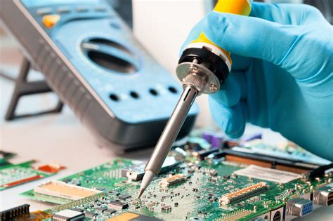
Tip 4: Replace Damaged Components
If a component on the PCB is damaged or malfunctioning, it may need to be replaced. This can be a delicate process, as it involves desoldering the old component and soldering a new one in its place. Here are some steps to replace a damaged component:
- Identify the damaged component and find a suitable replacement.
- Use a desoldering tool or solder wick to remove the old component from the board.
- Clean the area around the component pads with isopropyl alcohol.
- Place the new component in position, ensuring that it is oriented correctly.
- Solder the new component in place, being careful not to overheat or damage the board.
Desoldering Methods
There are several methods for desoldering components from a PCB:
| Method | Description |
|---|---|
| Desoldering pump | A manual tool that uses suction to remove molten solder from a joint |
| Desoldering wick | A braided copper wire that absorbs molten solder when heated |
| Desoldering station | An electric tool that combines a soldering iron with a vacuum pump for easy desoldering |
Soldering Tips
When soldering new components onto a PCB, there are a few tips to keep in mind:
- Use a temperature-controlled soldering iron set to the appropriate temperature for the solder being used.
- Use a small amount of solder, just enough to create a strong joint.
- Work quickly to avoid overheating the board or component.
- Use a magnifying glass or microscope to ensure accurate placement of small components.
Tip 5: Repair Damaged Pads
Pads are the small metal areas on a PCB where components are soldered. They can be damaged by overheating, physical trauma, or corrosion. If a pad is damaged, it can be difficult or impossible to solder a component to it securely. Here are some methods for repairing damaged pads:
Pad Repair Kit Method
A pad repair kit contains a small piece of copper-clad board and some epoxy adhesive. Here’s how to use a pad repair kit:
- Clean the area around the damaged pad with isopropyl alcohol.
- Cut a small piece of copper-clad board to fit over the damaged pad.
- Mix the epoxy adhesive according to the manufacturer’s instructions.
- Apply a small amount of adhesive to the back of the copper-clad board and place it over the damaged pad.
- Allow the adhesive to cure completely before soldering to the new pad.
Wire Jumper Method
If the damaged pad is small and isolated, a wire jumper can be used to connect the component to a nearby trace or pad. Here’s how to create a wire jumper:
- Clean the area around the damaged pad with isopropyl alcohol.
- Strip a small piece of insulated wire and tin the ends with solder.
- Solder one end of the wire to the component lead, and the other end to a nearby trace or pad.
- Trim any excess wire and ensure the connection is secure.
Tip 6: Test and Verify
After making any repairs to a PCB, it is important to test and verify that the board is functioning correctly. This can be done through visual inspection, continuity testing, and functional testing. Here are some steps to test and verify a repaired PCB:
- Visually inspect the board for any obvious issues such as loose components, broken traces, or solder bridges.
- Use a Multimeter to test for continuity between key points on the board, such as power and ground.
- Power on the board and test its functionality, either by connecting it to its intended device or using a test jig.
- If the board passes all tests, it can be considered repaired and ready for use.
Testing Equipment
There are several types of equipment that can be used to test and verify a PCB:
| Equipment | Description |
|---|---|
| Multimeter | A basic tool for measuring voltage, current, and resistance |
| Oscilloscope | A tool for visualizing and measuring electrical signals over time |
| Logic analyzer | A tool for capturing and analyzing digital signals |
| Functional tester | A specialized device for testing the specific functionality of a PCB |
Conclusion
Repairing a damaged PCB can be a complex and delicate process, but with the right tools and techniques, it is possible to restore a board to working condition. By following these six tips – identifying the problem, cleaning the board, repairing damaged traces, replacing damaged components, repairing damaged pads, and testing and verifying – you can successfully repair a wide range of PCB issues. Whether you are a hobbyist or a professional, learning how to repair PCBs can save you time and money, and give you a deeper understanding of how these essential components work.
Frequently Asked Questions
1. What tools do I need to repair a PCB?
To repair a PCB, you will need a few essential tools:
- Soldering iron and solder
- Desoldering pump or wick
- Multimeter
- Tweezers and pliers
- Magnifying glass or microscope
- Isopropyl alcohol and cleaning supplies
- Replacement components as needed
2. Can I repair a PCB without any experience?
While it is possible to repair some simple PCB issues without extensive experience, it is generally recommended to have some knowledge of electronics and soldering before attempting PCB repairs. If you are new to PCB repair, it may be best to start with simpler projects and work your way up to more complex repairs.
3. How do I know if a component needs to be replaced?
If a component is visibly damaged, such as being burnt or cracked, it will likely need to be replaced. You can also test components with a multimeter to check for proper function. If a component is not functioning within its specified parameters, it may need to be replaced.
4. Can I use regular glue to repair a PCB?
No, regular glue should not be used to repair a PCB. Most types of glue are not conductive and can actually insulate traces and pads, preventing proper electrical contact. If you need to attach something to a PCB, use a specialized adhesive such as epoxy or silicone.
5. How can I prevent PCB damage in the future?
To prevent PCB damage, it is important to handle boards carefully and protect them from physical damage, moisture, and electrostatic discharge. When storing PCBs, use anti-static bags or containers to prevent damage from static electricity. If a PCB will be exposed to harsh environments, consider applying a conformal coating to protect it from moisture and corrosion. Finally, always handle PCBs by the edges to avoid damaging components or traces.
No responses yet