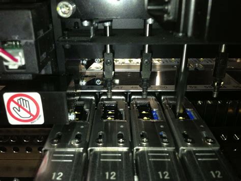
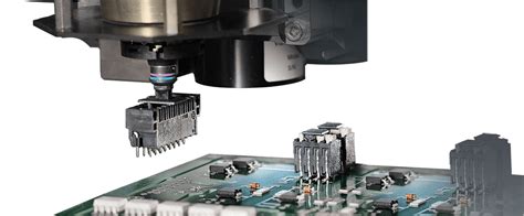
1. Component Selection and Placement
One of the most critical aspects of PCB assembly is the selection and placement of electronic components. It is essential to choose components that meet the design specifications, are of high quality, and are compatible with the PCB layout. The placement of components on the board should also be carefully considered to ensure optimal performance and minimize the risk of interference or signal integrity issues.
Factors to Consider in Component Selection
| Factor | Description |
|---|---|
| Functionality | The component must fulfill the required electrical and mechanical functions. |
| Quality | High-quality components from reputable manufacturers should be used to ensure reliability. |
| Compatibility | The component must be compatible with the PCB layout and other components on the board. |
| Cost | The cost of the component should be considered in relation to the overall budget of the project. |
Best Practices for Component Placement
- Follow the manufacturer’s recommended placement guidelines.
- Consider the component’s size, shape, and orientation.
- Ensure adequate spacing between components to avoid interference.
- Place sensitive components away from sources of heat or electromagnetic interference.
- Use automated placement machines for high-volume production to ensure consistency and accuracy.
2. Solder Paste Application
Solder paste is a mixture of tiny solder particles suspended in flux. It is applied to the PCB pads before the placement of components. The quality and consistency of the solder paste application are crucial for achieving reliable solder joints during the reflow process.
Solder Paste Application Methods
| Method | Description |
|---|---|
| Stencil Printing | A stencil with openings corresponding to the PCB pads is used to apply solder paste. |
| Dispensing | Solder paste is dispensed onto the PCB pads using a pneumatic or mechanical dispenser. |
| Jet Printing | A jet printer precisely deposits solder paste onto the PCB pads. |
Factors Affecting Solder Paste Application
- Stencil design and thickness
- Solder paste viscosity and composition
- Printing parameters (speed, pressure, separation distance)
- PCB pad design and surface finish
- Environmental conditions (temperature, humidity)
3. Reflow Soldering
Reflow soldering is the process of heating the PCB assembly to melt the solder paste and form permanent solder joints between the components and the PCB pads. The reflow process must be carefully controlled to ensure optimal solder joint formation and to prevent defects such as bridging, tombstoning, or insufficient wetting.
Reflow Soldering Profile
A typical reflow soldering profile consists of four stages:
- Preheat: The PCB is gradually heated to activate the flux and remove moisture.
- Soak: The temperature is maintained to allow the components to reach thermal equilibrium.
- Reflow: The temperature is raised above the melting point of the solder to form solder joints.
- Cooling: The PCB is cooled down to solidify the solder joints.
Factors Affecting Reflow Soldering
- Reflow profile parameters (temperature, time, ramp rates)
- Solder paste composition and quality
- Component thermal mass and sensitivity
- PCB design and thermal management
- Oven type and control system

4. Inspection and Testing
After the reflow soldering process, it is essential to inspect and test the PCB assembly to ensure that all solder joints are properly formed and that the components are functioning as intended. Various inspection and testing methods can be employed, depending on the complexity of the PCB and the required level of quality assurance.
Inspection Methods
| Method | Description |
|---|---|
| Visual Inspection | Manual or automated visual inspection of solder joints and component placement. |
| Automated Optical Inspection (AOI) | Uses cameras and image processing algorithms to detect defects. |
| X-Ray Inspection | Non-destructive inspection of solder joints under surface-mount components. |
Testing Methods
| Method | Description |
|---|---|
| In-Circuit Testing (ICT) | Verifies the correctness of the PCB assembly by testing individual components and circuits. |
| Functional Testing | Tests the PCB assembly under real-world operating conditions to ensure proper functionality. |
| Boundary Scan Testing | Uses built-in test circuitry to test the interconnections between components. |
5. Rework and Repair
Despite the best efforts to ensure a high-quality PCB assembly, defects or failures may still occur. In such cases, rework and repair techniques are employed to correct the issues and salvage the PCB.
Common Rework and Repair Techniques
- Desoldering and replacement of defective components
- Solder joint rework using soldering irons or hot air tools
- Pad repair using conductive epoxy or copper foil
- Trace repair using jumper wires or conductive ink
Best Practices for Rework and Repair
- Use the appropriate tools and techniques for the specific rework or repair task.
- Follow the manufacturer’s guidelines for component removal and replacement.
- Ensure proper cleaning and preparation of the rework area.
- Perform post-rework inspection and testing to verify the success of the repair.
6. Process Control and Documentation
To ensure consistent quality and repeatability in PCB assembly, it is crucial to establish and maintain proper process control and documentation. This includes defining and monitoring key process parameters, implementing quality control measures, and maintaining detailed records of the assembly process.
Elements of Process Control
- Defined and documented assembly procedures
- Regular calibration and maintenance of equipment
- Statistical process control (SPC) for key process parameters
- Traceability of materials and components
- Employee training and qualification
Documentation Requirements
- Bill of Materials (BOM)
- Assembly drawings and schematics
- Work instructions and standard operating procedures (SOPs)
- Inspection and test reports
- Rework and repair records
Frequently Asked Questions (FAQ)
1. What is the difference between through-hole and surface-mount PCB assembly?
Through-hole assembly involves inserting component leads through holes drilled in the PCB and soldering them on the opposite side. Surface-mount assembly involves placing components directly onto the PCB pads and soldering them in place. Surface-mount assembly allows for smaller components and higher density PCBs.
2. What are some common defects in PCB assembly?
Common defects in PCB assembly include:
– Bridging: Unintended solder connections between adjacent pads or traces.
– Tombstoning: One end of a component lifts off the PCB pad during reflow.
– Insufficient wetting: Solder does not fully cover the PCB pad or component lead.
– Component misalignment: Components are not placed accurately on the PCB pads.
3. How can I prevent electrostatic discharge (ESD) damage during PCB assembly?
To prevent ESD damage, follow these best practices:
– Use ESD-safe workstations, mats, and wrist straps.
– Store components and PCBs in ESD-safe packaging when not in use.
– Ensure proper grounding of personnel and equipment.
– Minimize handling of sensitive components.
4. What is the purpose of cleaning the PCB after soldering?
Cleaning the PCB after soldering helps remove flux residues, which can cause corrosion, leakage currents, or degradation of the solder joints over time. Cleaning also improves the appearance and facilitates inspection of the PCB assembly.
5. How do I select the appropriate solder paste for my PCB assembly?
When selecting solder paste, consider the following factors:
– Alloy composition: Choose a solder alloy that meets the requirements for melting temperature, strength, and compatibility with the components and PCB finish.
– Particle size: Select a particle size that is appropriate for the PCB pad dimensions and stencil thickness.
– Flux type: Choose a flux that provides adequate wetting and cleaning properties for your specific application and cleaning process.
– Viscosity: Ensure that the solder paste viscosity is suitable for the selected application method (e.g., stencil printing or dispensing).
In conclusion, paying attention to these six essential points in PCB assembly – component selection and placement, solder paste application, reflow soldering, inspection and testing, rework and repair, and process control and documentation – is crucial for ensuring a high-quality and reliable end product. By following best practices and maintaining a well-controlled assembly process, manufacturers can minimize defects, improve yield, and deliver PCBs that meet or exceed customer expectations.
No responses yet