Understanding PCB Hole Tolerance
When designing a printed circuit board (PCB), one of the critical aspects to consider is the hole size tolerance. PCB holes are used for various purposes, such as mounting components, facilitating electrical connections, and enabling mechanical fastening. Ensuring the correct hole size tolerance is essential for the proper functioning and reliability of the PCB.
What is PCB Hole Tolerance?
PCB hole tolerance refers to the acceptable range of variation in the diameter of holes drilled or punched in a PCB. It is the difference between the maximum and minimum allowable hole sizes. The tolerance is typically expressed as a plus or minus value, such as ±0.1mm or ±0.005 inches.
Why is PCB Hole Tolerance Important?
Specifying the appropriate PCB hole tolerance is crucial for several reasons:
-
Component Fitment: Holes that are too small may not allow components to be inserted properly, while holes that are too large may result in loose or poorly secured components.
-
Electrical Connectivity: Accurately sized holes ensure proper electrical connections between components and the PCB. Holes that are too small or too large can lead to poor or incomplete connections.
-
Manufacturing Feasibility: Overly tight tolerances may increase manufacturing complexity and cost, while excessively loose tolerances can compromise the quality and reliability of the PCB.
Tip 1: Consider the Component Requirements
When specifying PCB hole size tolerance, it is essential to consider the requirements of the components that will be mounted on the board. Different components have varying lead or pin sizes, and the hole tolerance should be selected accordingly.
Through-Hole Components
Through-hole components, such as resistors, capacitors, and connectors, have leads that are inserted into holes drilled in the PCB. The hole size tolerance should be chosen based on the lead diameter of the components.
| Component Lead Diameter | Recommended Hole Size Tolerance |
|---|---|
| 0.5mm – 0.8mm | ±0.1mm |
| 0.8mm – 1.0mm | ±0.15mm |
| 1.0mm – 1.5mm | ±0.2mm |
| 1.5mm – 2.0mm | ±0.25mm |
Surface Mount Components
Surface mount components, such as chip resistors and capacitors, do not require holes for mounting. However, some surface mount components, like BGA (Ball Grid Array) packages, have solder balls that need to align with pads on the PCB. In such cases, the pad size and spacing should be carefully considered to ensure proper soldering and component placement.

Tip 2: Understand the Manufacturing Process
The manufacturing process used to fabricate the PCB can influence the achievable hole size tolerance. Different manufacturing methods have varying capabilities and limitations.
Drilling
Drilling is the most common method for creating holes in PCBs. The accuracy and precision of the drilling process depend on factors such as the drill bit size, spindle speed, and material properties. Generally, smaller drill bits can achieve tighter tolerances compared to larger drill bits.
| Drill Bit Size | Typical Tolerance |
|---|---|
| 0.2mm – 0.5mm | ±0.05mm |
| 0.5mm – 1.0mm | ±0.1mm |
| 1.0mm – 2.0mm | ±0.15mm |
| 2.0mm – 3.0mm | ±0.2mm |
Punching
Punching is another method used for creating holes in PCBs, particularly for larger hole sizes or high-volume production. Punching involves using a die to punch out the desired hole shape. The achievable tolerance with punching depends on factors such as the die quality, material thickness, and punching force.
| Material Thickness | Typical Tolerance |
|---|---|
| 0.5mm – 1.0mm | ±0.1mm |
| 1.0mm – 1.5mm | ±0.15mm |
| 1.5mm – 2.0mm | ±0.2mm |

Tip 3: Allow for Plating Thickness
When specifying PCB hole size tolerance, it is important to account for the thickness of the plating that will be applied to the holes. Plating, such as copper or gold, is often used to improve electrical conductivity and protect the holes from corrosion.
The plating thickness can vary depending on the plating process and the desired performance characteristics. Typical plating thicknesses range from 25μm to 50μm (1 mil to 2 mil). When specifying the hole size tolerance, the plating thickness should be added to the nominal hole size to ensure that the plated hole meets the desired dimensions.
For example, if a nominal hole size of 1.0mm is required and the plating thickness is 50μm (2 mil), the hole size tolerance should be specified as 1.0mm +0.1/-0.05mm. This allows for the plating thickness while maintaining the desired hole size range.

Tip 4: Communicate Clearly with the Manufacturer
Clear communication with the PCB manufacturer is essential to ensure that the specified hole size tolerances are understood and achievable. Provide detailed specifications and drawings that clearly indicate the required hole sizes, tolerances, and any special requirements.
When communicating with the manufacturer, consider the following:
-
Use standard terminology: Use industry-standard terms and notations to specify hole sizes and tolerances. This helps avoid confusion and ensures that the manufacturer interprets the requirements correctly.
-
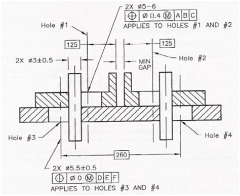
Provide detailed drawings: Include clear and accurate drawings that show the hole locations, sizes, and tolerances. Use appropriate dimensions and tolerancing methods, such as geometric dimensioning and tolerancing (GD&T), to convey the requirements precisely.
-
Discuss manufacturability: Engage in a dialogue with the manufacturer to discuss the feasibility and cost implications of the specified hole size tolerances. The manufacturer can provide valuable insights and recommendations based on their experience and capabilities.
Tip 5: Consider the Impact on Cost and Lead Time
Specifying tight hole size tolerances can have an impact on the cost and lead time of PCB fabrication. Tighter tolerances often require more precise manufacturing processes, specialized equipment, and additional quality control measures, which can increase the overall cost and lead time.
When specifying hole size tolerances, consider the following cost and lead time implications:
-
Manufacturing complexity: Tighter tolerances may require more advanced manufacturing techniques, such as laser drilling or precision punching, which can increase the complexity and cost of the fabrication process.
-
Quality control: Achieving tight tolerances necessitates stringent quality control measures, including frequent inspections and measurements. This additional quality control effort can add to the overall cost and lead time.
-
Material selection: The choice of PCB material can impact the achievable hole size tolerance. Some materials, such as high-performance or specialty laminates, may have different drilling or punching characteristics compared to standard FR-4 material. This can affect the cost and lead time of the PCB fabrication.
It is important to strike a balance between the required hole size tolerance and the associated cost and lead time implications. Discuss the trade-offs with the PCB manufacturer and consider relaxing the tolerances if they do not significantly impact the functionality or reliability of the PCB.
Frequently Asked Questions (FAQ)
-
What is the typical hole size tolerance for standard PCB designs?
The typical hole size tolerance for standard PCB designs is ±0.1mm (±4 mil). This tolerance is suitable for most through-hole components and provides a good balance between manufacturability and cost. However, the specific tolerance requirements may vary depending on the components and the PCB application. -
Can I specify different hole size tolerances for different parts of the PCB?
Yes, it is possible to specify different hole size tolerances for different parts of the PCB. This is often done when certain areas of the PCB have specific requirements, such as tighter tolerances for critical components or looser tolerances for non-critical areas. Clearly communicate the different tolerance requirements to the PCB manufacturer and provide detailed drawings to avoid confusion. -
What should I do if my components require tighter hole size tolerances than the manufacturer’s standard capabilities?
If your components require tighter hole size tolerances than the manufacturer’s standard capabilities, discuss the specific requirements with the manufacturer. They may be able to accommodate tighter tolerances using specialized equipment or processes. However, this may come at an additional cost and may impact the lead time. Consider alternative components or design adjustments if the cost and lead time implications are not feasible for your project. -
How do I ensure that the plated holes meet the specified tolerances?
To ensure that the plated holes meet the specified tolerances, consider the following: - Clearly communicate the plating requirements, including the plating thickness and any specific plating materials or processes.
- Specify the hole size tolerance taking into account the plating thickness. The nominal hole size should be adjusted to accommodate the plating while maintaining the desired hole size range.
- Request a plating thickness report or measurement data from the manufacturer to verify that the plating meets the specified requirements.
-
Perform incoming inspection or quality control checks on the received PCBs to ensure that the plated holes meet the specified tolerances.
-
Can I use the same hole size tolerance for all the holes on my PCB?
Using the same hole size tolerance for all the holes on a PCB is possible, but it may not always be the most optimal approach. Different components and mounting requirements may have varying hole size tolerance needs. It is recommended to assess the specific requirements of each component and specify the appropriate tolerances accordingly. This can help optimize the manufacturability, cost, and reliability of the PCB.
Conclusion
Specifying the appropriate PCB hole size tolerance is crucial for ensuring the proper functionality, reliability, and manufacturability of the PCB. By considering the component requirements, understanding the manufacturing process, allowing for plating thickness, communicating clearly with the manufacturer, and assessing the impact on cost and lead time, you can make informed decisions when specifying hole size tolerances.
Remember to strike a balance between the required tolerances and the associated manufacturing implications. Work closely with your PCB manufacturer to discuss the feasibility and optimize the design for successful fabrication.
By following these tips and guidelines, you can effectively specify PCB hole size tolerances that meet your project requirements while maintaining cost-effectiveness and manufacturability.

No responses yet