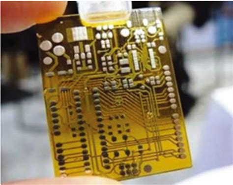
What is a 3D-Printed PCB?
A 3D-printed PCB, also known as a 3D-printed circuit board, is a printed circuit board that is manufactured using additive manufacturing techniques, specifically 3D printing technology. Unlike traditional PCB manufacturing methods, which involve subtractive processes like etching and drilling, 3D printing builds the circuit board layer by layer, depositing conductive and insulating materials as needed.
The process of creating a 3D-printed PCB begins with designing the circuit using computer-aided design (CAD) software. The CAD file is then converted into a format compatible with the 3D printer, such as STL (Standard Tessellation Language) or AMF (Additive Manufacturing File). The 3D printer then builds the PCB by depositing the necessary materials, typically conductive filaments or inks, onto a substrate according to the design.
Advantages of 3D-Printed PCBs
1. Rapid Prototyping
One of the most significant advantages of 3D-printed PCBs is the ability to create prototypes quickly and efficiently. Traditional PCB manufacturing methods often require a considerable amount of time and resources, especially for complex designs or small production runs. With 3D printing, designers can create functional prototypes within hours, allowing for faster iteration and testing of new ideas.
2. Cost-Effectiveness
3D printing technology has the potential to reduce the overall cost of PCB production, particularly for low-volume runs or custom designs. Traditional PCB manufacturing methods often require high setup costs and minimum order quantities, making them less cost-effective for small-scale production. 3D printing eliminates the need for expensive tooling and allows for on-demand production, reducing waste and inventory costs.
3. Design Flexibility
3D-printed PCBs offer unparalleled design flexibility compared to traditional manufacturing methods. With additive manufacturing, designers can create complex geometries, curved surfaces, and embedded components that would be challenging or impossible to achieve with subtractive processes. This freedom of design enables the creation of more compact, lightweight, and functionally integrated PCBs.
4. Customization
3D printing technology allows for easy customization of PCBs, catering to specific application requirements. Designers can modify the circuit layout, component placement, and even the materials used to optimize the PCB’s performance, durability, or thermal properties. This level of customization is particularly beneficial for industries that require specialized or application-specific electronics.

Limitations of 3D-Printed PCBs
Despite the numerous advantages of 3D-printed PCBs, there are still some limitations that need to be addressed:
1. Material Properties
Currently, the range of materials available for 3D printing PCBs is limited compared to traditional manufacturing methods. While conductive filaments and inks have been developed, their electrical and thermal properties may not match those of copper traces used in conventional PCBs. This can impact the performance and reliability of 3D-printed PCBs in certain applications.
2. Resolution and Accuracy
The resolution and accuracy of 3D-printed PCBs are dependent on the capabilities of the 3D printer and the materials used. While advancements in 3D printing technology have improved the precision of printed traces and components, they may still fall short of the high-resolution features achievable through traditional manufacturing methods. This can limit the complexity and density of 3D-printed PCBs.
3. Production Speed
Although 3D printing enables rapid prototyping, the production speed for larger volumes of PCBs may be slower compared to traditional manufacturing methods. The layer-by-layer deposition process can be time-consuming, especially for complex designs or thicker PCBs. This limitation may restrict the use of 3D-printed PCBs for high-volume production runs.
4. Post-Processing Requirements
3D-printed PCBs often require post-processing steps to improve their functionality and durability. These steps may include curing, polishing, or coating the PCB to enhance its electrical conductivity, insulation, or surface finish. Additionally, components still need to be manually soldered onto the 3D-printed PCB, which can be a time-consuming process.

Applications of 3D-Printed PCBs
Despite the current limitations, 3D-printed PCBs have already found applications in various industries:
1. Prototyping and Product Development
3D-printed PCBs are widely used for rapid prototyping and product development. They allow designers to quickly test and refine their ideas, reducing the time and cost associated with traditional prototyping methods. This is particularly valuable in industries such as consumer electronics, automotive, and aerospace, where faster time-to-market is crucial.
2. Wearable Electronics
The design flexibility offered by 3D printing has made it an attractive option for creating wearable electronics. 3D-printed PCBs can be designed to conform to the shape of the human body, enabling the integration of sensors, antennas, and other components into clothing, accessories, or medical devices. This has applications in healthcare, fitness, and fashion industries.
3. Internet of Things (IoT) Devices
3D-printed PCBs can be used to create custom IoT devices, such as sensors, actuators, and communication modules. The ability to embed components and create complex geometries makes 3D printing well-suited for designing compact and lightweight IoT devices. This is particularly relevant for applications in smart homes, industrial automation, and environmental monitoring.
4. Education and Hobbyist Projects
3D-printed PCBs have also found a place in education and hobbyist projects. They provide an accessible and affordable way for students and enthusiasts to learn about electronics and create their own custom circuits. Many educational institutions and maker spaces have incorporated 3D printing technology into their curriculum and facilities, fostering innovation and hands-on learning.

Future Prospects and Research
As 3D printing technology continues to evolve, the potential applications and capabilities of 3D-printed PCBs are expected to expand. Researchers and industry experts are actively working on developing new materials, improving printing resolution, and optimizing the manufacturing process to overcome the current limitations.
One area of research is the development of multi-material 3D printing, which would allow for the simultaneous deposition of conductive and insulating materials, enabling the creation of more complex and integrated PCBs. Advancements in conductive inks and filaments are also being made to improve their electrical and thermal properties, bringing them closer to the performance of traditional PCB materials.
Another promising avenue is the integration of 3D printing with other manufacturing technologies, such as pick-and-place machines for component assembly. This hybrid approach could streamline the production process, reducing the need for manual post-processing steps and enabling faster turnaround times.
As the technology matures, it is expected that 3D-printed PCBs will find wider adoption across various industries, particularly in applications that require customization, rapid prototyping, or complex geometries. The ability to create functional electronics on-demand and in-house could revolutionize the way we design and manufacture electronic devices.
Frequently Asked Questions (FAQ)
1. What materials are used to create 3D-printed PCBs?
3D-printed PCBs are typically created using conductive filaments or inks, such as those based on silver, copper, or graphene. These materials are deposited onto a substrate, such as plastic or resin, to form the conductive traces and components of the PCB.
2. Can 3D-printed PCBs replace traditional PCBs in all applications?
Currently, 3D-printed PCBs may not be suitable for all applications, especially those that require high-volume production, strict performance requirements, or complex designs. Traditional PCB manufacturing methods still offer advantages in terms of material properties, resolution, and production speed. However, as 3D printing technology advances, it is expected to become a viable alternative for a wider range of applications.
3. What are the key challenges in adopting 3D-printed PCBs?
Some of the key challenges in adopting 3D-printed PCBs include limited material options, lower resolution and accuracy compared to traditional manufacturing methods, slower production speeds for larger volumes, and the need for post-processing steps. Addressing these challenges through research and development will be crucial for the widespread adoption of 3D-printed PCBs.
4. How does the cost of 3D-printed PCBs compare to traditional PCBs?
The cost comparison between 3D-printed PCBs and traditional PCBs depends on various factors, such as the complexity of the design, the volume of production, and the specific materials used. For low-volume runs or custom designs, 3D-printed PCBs can be more cost-effective due to the elimination of tooling costs and the ability to produce on-demand. However, for high-volume production, traditional PCB manufacturing methods may still offer cost advantages.
5. What are the potential environmental benefits of 3D-printed PCBs?
3D-printed PCBs have the potential to reduce waste and environmental impact compared to traditional manufacturing methods. Additive manufacturing processes generate less waste material, as they only deposit the necessary amount of material required for the PCB. Additionally, the ability to produce PCBs on-demand can reduce inventory waste and transportation emissions associated with traditional supply chains. However, the environmental impact of 3D printing materials and energy consumption should also be considered when assessing the overall sustainability of 3D-printed PCBs.
Conclusion
The emergence of 3D-printed PCBs represents a significant step forward in the electronics manufacturing industry. With the ability to create functional circuit boards using additive manufacturing processes, designers and manufacturers can benefit from faster prototyping, cost-effectiveness, design flexibility, and customization. While there are still limitations to overcome, such as material properties, resolution, and production speed, ongoing research and development efforts are aimed at addressing these challenges.
As 3D printing technology continues to evolve, it is expected to play an increasingly important role in the production of electronic devices across various industries. From rapid prototyping and wearable electronics to IoT devices and educational projects, 3D-printed PCBs have the potential to revolutionize the way we design and manufacture electronics.
By embracing this innovative technology and investing in further research and development, the electronics industry can unlock new possibilities, drive innovation, and create more sustainable and efficient manufacturing processes. The future of 3D-printed PCBs looks promising, and it will be exciting to witness the advancements and applications that emerge in the coming years.
No responses yet