Table of Contents
- 2N3904 Overview
- 2N3904 Datasheet Specifications
- Absolute Maximum Ratings
- Electrical Characteristics
- 2N3904 Pin Configuration and Package
- 2N3904 Applications
- Amplifier Circuits
- Switching Circuits
- Logic Gates
- Oscillator Circuits
- 2N3904 Biasing and Operating Modes
- Common Emitter Configuration
- Common Collector Configuration
- Common Base Configuration
- 2N3904 vs Other Transistors
- Handling and Soldering Precautions
- Frequently Asked Questions (FAQ)
- Conclusion
2N3904 Overview
The 2N3904 is a small-signal NPN transistor designed for general-purpose applications. It is known for its high current gain, low collector-emitter saturation voltage, and fast switching speeds. The transistor is widely available and can be found in various package types, including TO-92, SOT-23, and surface mount packages.

2N3904 Datasheet Specifications
To effectively use the 2N3904 transistor in your designs, it is crucial to understand its datasheet specifications. The following tables summarize the key parameters from the 2N3904 datasheet.
Absolute Maximum Ratings
| Parameter | Symbol | Value | Unit |
|---|---|---|---|
| Collector-Base Voltage | VCBO | 60 | V |
| Collector-Emitter Voltage | VCEO | 40 | V |
| Emitter-Base Voltage | VEBO | 6 | V |
| Collector Current | IC | 200 | mA |
| Total Power Dissipation | PD | 625 | mW |
| Operating Temperature Range | TJ | -55 to 150 | °C |
| Storage Temperature Range | Tstg | -55 to 150 | °C |
Electrical Characteristics
| Parameter | Symbol | Test Conditions | Min | Typ | Max | Unit |
|---|---|---|---|---|---|---|
| Collector-Emitter Saturation Voltage | VCE(sat) | IC = 10 mA, IB = 1 mA | – | 0.2 | 0.4 | V |
| Collector-Emitter Cutoff Voltage | VCE(off) | VBE = 0 V, IC = 1 µA | 40 | – | – | V |
| DC Current Gain | hFE | IC = 0.1 mA, VCE = 1 V | 40 | – | 300 | – |
| IC = 1 mA, VCE = 1 V | 70 | – | – | – | ||
| IC = 10 mA, VCE = 1 V | 100 | – | 300 | – | ||
| IC = 50 mA, VCE = 1 V | 60 | – | – | – | ||
| Collector-Base Cutoff Current | ICBO | VCB = 50 V, IE = 0 | – | – | 50 | nA |
| Emitter-Base Cutoff Current | IEBO | VEB = 3 V, IC = 0 | – | – | 50 | nA |
| Transition Frequency | fT | IC = 10 mA, VCE = 20 V, f = 100 MHz | 250 | 300 | – | MHz |

2N3904 Pin Configuration and Package
The 2N3904 transistor is available in various package types, with the most common being the TO-92 through-hole package. The pin configuration for the TO-92 package is as follows:
- Emitter
- Base
- Collector
It is essential to identify the correct pin configuration when designing circuits with the 2N3904 transistor to ensure proper functionality.

2N3904 Applications
The versatility of the 2N3904 transistor makes it suitable for a wide range of applications. Some common uses include:
Amplifier Circuits
The 2N3904 can be used as a small-Signal amplifier in various configurations, such as common emitter, common collector, and common base. These amplifiers can be used in audio, video, and RF applications.
Switching Circuits
Due to its fast switching speeds and low saturation voltage, the 2N3904 is well-suited for use in switching circuits. It can be used to control relays, motors, and other loads in response to input signals.
Logic Gates
The 2N3904 can be used to construct basic logic gates, such as AND, OR, and NOT gates. These logic gates can be combined to create more complex digital circuits.
Oscillator Circuits
The 2N3904 can be used in oscillator circuits to generate periodic waveforms. Common oscillator configurations include the Colpitts oscillator, Hartley oscillator, and crystal oscillator.
2N3904 Biasing and Operating Modes
To properly use the 2N3904 transistor in various applications, it is essential to understand its biasing and operating modes.
Common Emitter Configuration
In the common emitter configuration, the emitter is connected to ground, the input signal is applied to the base, and the output is taken from the collector. This configuration provides high current gain and voltage gain, making it suitable for amplifier applications.
Common Collector Configuration
Also known as an emitter follower, the common collector configuration has the collector connected to the power supply, the input signal applied to the base, and the output taken from the emitter. This configuration provides high input impedance, low output impedance, and a voltage gain of approximately 1.
Common Base Configuration
In the common base configuration, the base is connected to ground, the input signal is applied to the emitter, and the output is taken from the collector. This configuration provides high voltage gain and low input impedance, making it suitable for high-frequency applications.
2N3904 vs Other Transistors
When choosing a transistor for a specific application, it is essential to compare the 2N3904 with other similar transistors. Some common alternatives to the 2N3904 include:
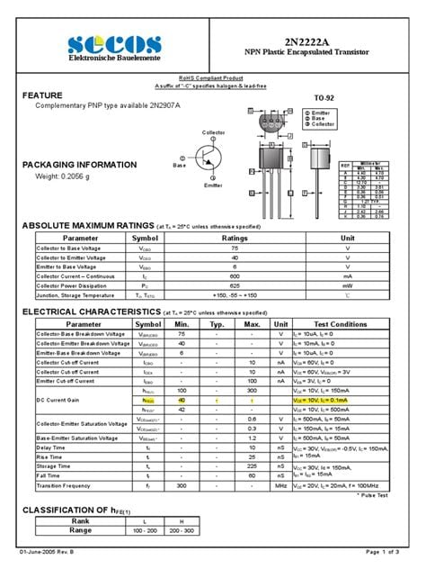
- 2N2222: Another popular NPN transistor with slightly higher maximum ratings than the 2N3904.
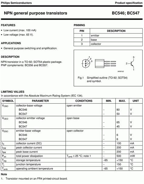
- BC547: An NPN transistor with similar characteristics to the 2N3904, often used in European designs.
- 2N4401: An NPN transistor with higher maximum ratings and higher current gain than the 2N3904.
The choice of transistor depends on the specific requirements of the application, such as power dissipation, current gain, and switching speed.
Handling and Soldering Precautions
When working with the 2N3904 transistor, it is essential to follow proper handling and soldering precautions to prevent damage to the device:
- Use a grounded anti-static wrist strap or work on an anti-static mat to prevent electrostatic discharge (ESD) damage.
- Avoid touching the leads of the transistor directly with your fingers, as oils and moisture can affect the device’s performance.
- Use a temperature-controlled soldering iron with a fine tip to avoid overheating the transistor during soldering.
- Follow the manufacturer’s recommended soldering profile, including temperature and duration, to ensure proper soldering without damaging the device.
Frequently Asked Questions (FAQ)
-
What is the maximum collector current for the 2N3904 transistor?
The maximum collector current for the 2N3904 transistor is 200 mA, as specified in the absolute maximum ratings table of the datasheet. -
Can the 2N3904 be used as a switch?
Yes, the 2N3904 can be used as a switch in various applications due to its fast switching speeds and low saturation voltage. -
What is the typical DC current gain (hFE) for the 2N3904?
The typical DC current gain (hFE) for the 2N3904 ranges from 100 to 300, depending on the collector current and collector-emitter voltage, as specified in the electrical characteristics table of the datasheet. -
What is the difference between the 2N3904 and the 2N2222 transistor?
The main difference between the 2N3904 and the 2N2222 is that the 2N2222 has slightly higher maximum ratings, such as a higher maximum collector-emitter voltage (VCEO) of 60 V compared to 40 V for the 2N3904. -
How can I prevent damage to the 2N3904 during handling and soldering?
To prevent damage to the 2N3904 during handling and soldering, use a grounded anti-static wrist strap or work on an anti-static mat, avoid touching the leads directly with your fingers, use a temperature-controlled soldering iron with a fine tip, and follow the manufacturer’s recommended soldering profile.
Conclusion
The 2N3904 transistor is a versatile and widely used NPN bipolar junction transistor suitable for a wide range of low-power amplifying and switching applications. By understanding the key specifications, pin configuration, biasing, and operating modes outlined in the 2N3904 datasheet, engineers and hobbyists can effectively utilize this transistor in their designs. When selecting a transistor for a specific application, it is essential to compare the 2N3904 with other similar transistors and consider factors such as power dissipation, current gain, and switching speed. Proper handling and soldering precautions must be followed to ensure the longevity and optimal performance of the 2N3904 transistor in your projects.

No responses yet