Introduction to PCB Stackup
In the world of high-density interconnect (HDI) printed circuit boards (PCBs), the stackup design plays a crucial role in determining the overall performance, reliability, and manufacturability of the board. A PCB stackup refers to the arrangement of copper layers, dielectric materials, and other components that make up the structure of a PCB. In this article, we will dive deep into the 2n2 PCB stackup design for HDI boards, exploring its benefits, considerations, and best practices.
What is a 2n2 PCB Stackup?
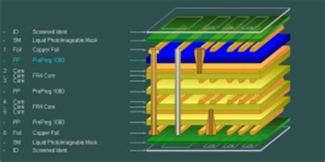
A 2n2 PCB stackup is a specific configuration that consists of two signal layers and two power/ground planes. The term “2n2” refers to the arrangement of these layers, with “2” representing the two signal layers and “n” indicating the presence of power/ground planes between them. This stackup design is commonly used in HDI boards due to its ability to provide a balance between signal integrity, power distribution, and manufacturability.
Benefits of 2n2 PCB Stackup
-
Improved Signal Integrity: The 2n2 stackup design helps minimize crosstalk and electromagnetic interference (EMI) by providing dedicated power/ground planes that act as shields between the signal layers. This arrangement reduces the coupling between signal traces and improves overall signal integrity.
-
Enhanced Power Distribution: With dedicated power/ground planes, the 2n2 stackup ensures a low-impedance power distribution network. This helps reduce voltage drops, minimize power supply noise, and improve the overall power integrity of the HDI board.
-
Simplified Manufacturing: Compared to more complex stackups, the 2n2 design simplifies the manufacturing process. It reduces the number of layers required, making it easier to fabricate and assemble the HDI board. This can lead to lower manufacturing costs and faster turnaround times.
-
Increased Flexibility: The 2n2 stackup provides flexibility in terms of routing and component placement. With two signal layers available, designers have more freedom to route traces and position components optimally, facilitating better signal routing and improved board layout.
Considerations for 2n2 PCB Stackup Design
When designing a 2n2 PCB stackup for HDI boards, several key considerations need to be taken into account to ensure optimal performance and manufacturability.
Material Selection
The choice of dielectric materials plays a significant role in the performance of the HDI board. The most commonly used materials for HDI applications include:
| Material | Dielectric Constant | Loss Tangent | Thermal Stability |
|---|---|---|---|
| FR-4 | 4.2 – 4.5 | 0.02 | Good |
| Polyimide | 3.2 – 3.5 | 0.002 – 0.003 | Excellent |
| Rogers | 2.2 – 10.2 | 0.0009 – 0.003 | Excellent |
When selecting the dielectric material, consider factors such as the operating frequency, signal speed, and thermal requirements of the HDI board. High-speed designs may benefit from materials with lower dielectric constants and loss tangents, such as polyimide or Rogers materials.
Layer Thickness and Spacing
The thickness of the copper layers and the spacing between them impact the electrical characteristics of the HDI board. Thinner copper layers are preferred for HDI designs to achieve finer trace widths and smaller via sizes. However, the copper thickness must be sufficient to handle the required current carrying capacity.
The spacing between layers, known as the dielectric thickness, affects the impedance and capacitance of the traces. Thinner dielectrics allow for higher trace densities but may increase the risk of signal integrity issues. It is important to strike a balance between layer spacing and signal integrity requirements.
Via Technology
HDI boards often employ advanced via technologies to achieve high interconnect density. The choice of via technology depends on the design requirements and manufacturing capabilities. Some common via types used in HDI designs include:
-
Microvia: These are small, laser-drilled vias that connect the outer layers to the inner layers. Microvias have diameters typically ranging from 50 to 150 microns and are used for high-density interconnects.
-
Buried Via: Buried vias are used to connect inner layers within the PCB stackup. They are not visible from the outer surfaces of the board and are created during the lamination process.
-
Blind Via: Blind vias connect an outer layer to one or more inner layers but do not penetrate through the entire thickness of the board. They are drilled from one side of the board and terminate at a specific inner layer.
The selection of via technology depends on factors such as the required interconnect density, signal integrity, and manufacturing capabilities.
Signal Integrity Analysis
To ensure the optimal performance of the HDI board, it is crucial to perform signal integrity analysis during the design phase. Signal integrity simulations help identify potential issues related to crosstalk, impedance mismatches, and reflections. By analyzing the signal behavior in the 2n2 stackup, designers can make necessary adjustments to the layout, trace widths, and spacing to mitigate signal integrity problems.

Best Practices for 2n2 PCB Stackup Design
To achieve a robust and reliable 2n2 PCB stackup for HDI boards, consider the following best practices:
-
Use symmetric stackup: Maintain symmetry in the stackup design by placing the signal layers and power/ground planes in a balanced manner. This helps minimize warpage and improves the mechanical stability of the board.
-
Minimize signal layer changes: Avoid frequent layer changes for signal traces to reduce the number of vias required. Minimize the use of blind and buried vias when possible to simplify the manufacturing process.
-
Provide adequate power and ground planes: Ensure that the power and ground planes have sufficient copper coverage to provide a low-impedance power distribution network. Use multiple power and ground planes if necessary to meet the power requirements of the HDI board.
-
Control impedance: Maintain consistent impedance throughout the signal paths by carefully selecting the trace widths, spacing, and dielectric materials. Perform impedance calculations and simulations to ensure that the desired impedance targets are met.
-
Implement proper grounding and shielding: Use ground planes and shielding techniques to minimize EMI and crosstalk. Implement proper grounding strategies, such as creating separate analog and digital ground planes, to prevent ground loops and reduce noise.
-
Follow manufacturing guidelines: Adhere to the manufacturing guidelines provided by the PCB fabricator to ensure the manufacturability of the 2n2 stackup. Consider the minimum trace widths, spacing, and via sizes that can be reliably manufactured.
FAQ
-
Q: What is the main advantage of using a 2n2 PCB stackup for HDI boards?
A: The main advantage of a 2n2 PCB stackup for HDI boards is the balance it provides between signal integrity, power distribution, and manufacturability. The dedicated power/ground planes help improve signal integrity and power distribution, while the simplified structure makes manufacturing easier and more cost-effective. -
Q: Can a 2n2 PCB stackup be used for high-speed designs?
A: Yes, a 2n2 PCB stackup can be used for high-speed designs. However, careful consideration must be given to the choice of dielectric materials, layer thicknesses, and spacing to ensure optimal signal integrity. High-speed designs may benefit from using low-loss materials and thin dielectrics to minimize signal degradation. -
Q: What are the common via technologies used in 2n2 PCB stackups for HDI boards?
A: The common via technologies used in 2n2 PCB stackups for HDI boards include microvias, buried vias, and blind vias. Microvias are small, laser-drilled vias used for high-density interconnects. Buried vias connect inner layers within the stackup, while blind vias connect an outer layer to one or more inner layers without penetrating through the entire board thickness. -
Q: How does signal integrity analysis help in the design of 2n2 PCB stackups?
A: Signal integrity analysis helps identify potential issues related to crosstalk, impedance mismatches, and reflections in the 2n2 PCB stackup. By performing simulations and analyzing the signal behavior, designers can make necessary adjustments to the layout, trace widths, and spacing to mitigate signal integrity problems and ensure optimal performance of the HDI board. -
Q: What are some best practices for designing a 2n2 PCB stackup for HDI boards?
A: Some best practices for designing a 2n2 PCB stackup for HDI boards include using a symmetric stackup, minimizing signal layer changes, providing adequate power and ground planes, controlling impedance, implementing proper grounding and shielding techniques, and following manufacturing guidelines. These practices help ensure a robust, reliable, and manufacturable HDI board.
Conclusion
The 2n2 PCB stackup design is a popular choice for HDI boards due to its ability to provide a balance between signal integrity, power distribution, and manufacturability. By carefully considering factors such as material selection, layer thickness and spacing, via technology, and signal integrity analysis, designers can create a robust and reliable 2n2 stackup that meets the specific requirements of their HDI board.
Following best practices such as using a symmetric stackup, minimizing signal layer changes, providing adequate power and ground planes, controlling impedance, implementing proper grounding and shielding, and adhering to manufacturing guidelines can further enhance the performance and manufacturability of the HDI board.
As HDI technology continues to advance, the importance of optimizing the PCB stackup design becomes increasingly critical. By understanding the intricacies of 2n2 PCB stackups and applying the principles discussed in this article, designers can create high-performance HDI boards that meet the demands of modern electronic devices.
No responses yet