Introduction
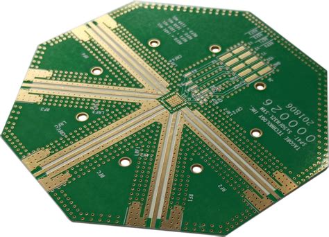
Immersion gold plating is a widely used surface finish for printed circuit boards (PCBs) in the electronics industry. This process involves depositing a thin layer of gold over a nickel substrate on the exposed copper pads of a PCB. Immersion gold offers numerous benefits that make it an attractive choice for manufacturers and designers alike. In this article, we will explore 13 key advantages of using immersion gold plating for PCBs.
What is Immersion Gold Plating?
Immersion gold plating, also known as electroless nickel immersion gold (ENIG), is a chemical process that deposits a thin layer of gold onto the exposed copper pads of a PCB. The process begins with the deposition of a nickel layer, which acts as a barrier between the copper and the gold. The nickel layer prevents the diffusion of copper into the gold, which could otherwise lead to the formation of intermetallic compounds that can degrade the solderability of the PCB.
Once the nickel layer is in place, the PCB is immersed in a gold plating solution. The gold ions in the solution are reduced and deposited onto the nickel surface through an autocatalytic reaction. The resulting gold layer is typically between 0.05 and 0.2 microns thick, providing excellent solderability and protection against oxidation.
The Immersion Gold Plating Process
| Step | Description |
|---|---|
| 1 | Clean and prepare the PCB surface |
| 2 | Deposit a thin layer of nickel (typically 3-6 microns) |
| 3 | Immerse the PCB in a gold plating solution |
| 4 | Gold ions are reduced and deposited onto the nickel surface |
| 5 | Rinse and dry the PCB |
Advantages of Immersion Gold Plating
1. Excellent Solderability
One of the primary advantages of immersion gold plating is its excellent solderability. The gold layer provides a clean, oxide-free surface that allows for easy and reliable soldering of components to the PCB. This is particularly important for surface mount technology (SMT) components, which require precise and consistent solder joints.
2. Long Shelf Life
Immersion gold plated PCBs have a long shelf life compared to other surface finishes. The gold layer protects the underlying copper from oxidation, ensuring that the PCB remains solderable even after extended storage periods. This is particularly beneficial for manufacturers who need to store PCBs for long periods before assembly.
3. Corrosion Resistance
Gold is a highly stable and corrosion-resistant metal. Immersion gold plating provides excellent protection against corrosion, even in harsh environments. This makes it an ideal choice for PCBs that will be used in industrial, automotive, or aerospace applications, where reliability and durability are critical.
4. Compatibility with Multiple Soldering Processes
Immersion gold plating is compatible with a wide range of soldering processes, including reflow soldering, wave soldering, and hand soldering. This versatility makes it a popular choice for manufacturers who use different soldering techniques for different products or applications.
5. Suitable for High-Density Layouts
As electronic devices become smaller and more complex, PCBs with high-density layouts are becoming increasingly common. Immersion gold plating is well-suited for these designs, as it provides a smooth, flat surface that allows for precise placement of small components. The thin gold layer also minimizes the risk of bridging between closely spaced pads.
6. Improved Wire Bonding
Immersion gold plating is an excellent choice for PCBs that require wire bonding. The gold surface provides a clean, oxide-free substrate for wire bonding, ensuring strong and reliable connections between the PCB and the bonded wires. This is particularly important for high-reliability applications, such as aerospace and medical devices.
7. Reduced Contact Resistance
The gold layer in immersion gold plating provides a low contact resistance between the PCB pads and the components. This is important for applications that require high electrical performance, such as high-speed digital circuits or sensitive analog circuits. The low contact resistance also helps to minimize signal loss and improve overall system performance.
8. Compatibility with Lead-Free Soldering
As environmental regulations become more stringent, lead-free soldering has become increasingly common in the electronics industry. Immersion gold plating is fully compatible with lead-free soldering processes, making it a suitable choice for manufacturers who need to comply with these regulations.
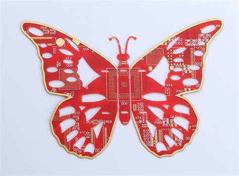
9. Aesthetically Pleasing Finish
In addition to its technical benefits, immersion gold plating also provides an aesthetically pleasing finish to PCBs. The gold layer gives the PCB a clean, professional appearance that can enhance the perceived quality of the final product. This can be particularly important for consumer electronics or other products where visual appeal is a key consideration.
10. Cost-Effective for High-Reliability Applications
While immersion gold plating may be more expensive than some other surface finishes, it is often a cost-effective choice for high-reliability applications. The long shelf life, excellent solderability, and corrosion resistance of immersion gold can help to reduce manufacturing defects and improve product reliability, ultimately leading to lower overall costs.
11. Suitable for Controlled Impedance Designs
Immersion gold plating is well-suited for PCBs with controlled impedance designs, such as high-speed digital circuits or RF applications. The thin, uniform gold layer minimally impacts the impedance of the PCB traces, ensuring that the desired impedance values are maintained.
12. Compatibility with Solder Masks
Immersion gold plating is compatible with a wide range of solder masks, including liquid photoimageable (LPI) and dry film solder masks. This flexibility allows manufacturers to choose the most appropriate solder mask for their specific application, without compromising the benefits of immersion gold plating.
13. RoHS Compliant
Immersion gold plating is compliant with the Restriction of Hazardous Substances (RoHS) directive, which restricts the use of certain hazardous materials in electronic products. This makes it a suitable choice for manufacturers who need to comply with RoHS regulations in order to sell their products in certain markets.

Frequently Asked Questions (FAQ)
1. What is the typical thickness of the gold layer in immersion gold plating?
The typical thickness of the gold layer in immersion gold plating ranges from 0.05 to 0.2 microns (2-8 microinches).
2. How does immersion gold plating differ from electroplated gold?
Immersion gold plating is an electroless process that relies on an autocatalytic reaction to deposit the gold layer, whereas electroplated gold involves the use of an electric current to deposit the gold. Immersion gold typically results in a thinner, more uniform gold layer compared to electroplated gold.
3. Can immersion gold plated PCBs be reworked?
Yes, immersion gold plated PCBs can be reworked. However, care must be taken to avoid damaging the thin gold layer during the rework process. It is recommended to use low-temperature soldering techniques and to minimize the time the PCB is exposed to high temperatures.
4. Is immersion gold plating suitable for press-fit connectors?
Yes, immersion gold plating is suitable for press-fit connectors. The smooth, hard surface of the gold layer provides an excellent substrate for press-fit connections, ensuring reliable and stable mechanical and electrical connections.
5. How does the cost of immersion gold plating compare to other surface finishes?
Immersion gold plating is generally more expensive than other surface finishes, such as HASL (Hot Air Solder Leveling) or OSP (Organic Solderability Preservative). However, the long-term benefits of immersion gold, such as improved reliability and longer shelf life, can often justify the higher initial cost for high-reliability applications.
Conclusion
Immersion gold plating offers a wide range of advantages for PCBs in the electronics industry. Its excellent solderability, long shelf life, corrosion resistance, and compatibility with various soldering processes make it a popular choice for manufacturers and designers. Additionally, immersion gold is well-suited for high-density layouts, wire bonding, and controlled impedance designs, making it a versatile surface finish for a wide range of applications.
While immersion gold plating may have a higher initial cost compared to other surface finishes, its long-term benefits can often justify the investment, particularly for high-reliability applications. As the electronics industry continues to evolve, with a focus on miniaturization, high performance, and environmental compliance, immersion gold plating is likely to remain a key surface finish for PCBs in the years to come.
No responses yet