1. Poor Design and Layout
One of the primary reasons for PCB manufacturing defects is poor design and layout. A well-designed PCB layout is crucial for ensuring the proper functioning of the circuit and minimizing the risk of defects. Common design and layout issues include:
- Inadequate clearance between components and traces
- Incorrect trace width and spacing
- Improper component placement
- Insufficient copper pour and grounding
Solutions:
- Use PCB design software with built-in design rule checks (DRC) to identify and correct layout issues.
- Follow industry-standard design guidelines and best practices.
- Collaborate with experienced PCB designers and manufacturers to optimize the layout.
- Conduct thorough design reviews and simulations to identify potential issues before manufacturing.
2. Incorrect Material Selection
Selecting the right materials for PCB manufacturing is essential for ensuring the reliability and performance of the final product. Using incorrect or subpar materials can lead to various defects, such as:
- Delamination
- Warping
- Reduced thermal and electrical conductivity
- Compatibility issues with soldermask and silkscreen
Solutions:
- Choose high-quality, industry-standard materials from reputable suppliers.
- Consider the specific requirements of your application, such as temperature, humidity, and mechanical stress.
- Work with experienced PCB manufacturers who can recommend suitable materials based on your needs.
- Conduct material testing and qualification to ensure compliance with specifications.
3. Manufacturing Process Inconsistencies
Inconsistencies in the PCB manufacturing process can introduce various defects, affecting the quality and reliability of the final product. Some common process inconsistencies include:
- Uneven etching
- Inadequate plating thickness
- Incorrect drill sizes and locations
- Insufficient solder mask coverage
Solutions:
- Implement strict process control measures and standard operating procedures (SOPs) to ensure consistency.
- Regularly calibrate and maintain manufacturing equipment to minimize variations.
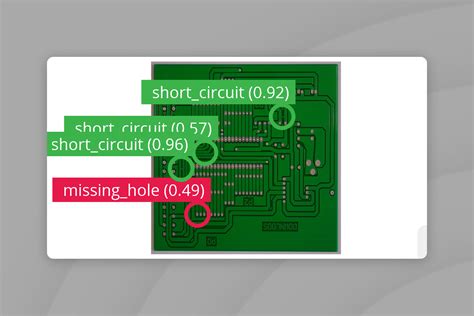
- Use automated inspection systems, such as automated optical inspection (AOI) and X-ray inspection, to detect process inconsistencies.
- Conduct regular audits and training sessions to ensure adherence to best practices.

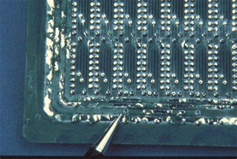
4. Contamination and Impurities
Contamination and impurities can be introduced during various stages of PCB manufacturing, leading to defects such as:
- Shorts and opens
- Reduced adhesion of soldermask and silkscreen
- Copper oxidation
- Plating defects
Solutions:
- Maintain a clean and controlled manufacturing environment with proper air filtration and humidity control.
- Use high-purity chemicals and materials to minimize the risk of contamination.
- Implement strict handling and storage procedures to prevent cross-contamination.
- Conduct regular contamination testing and analysis to identify and address potential sources.
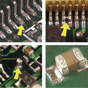
5. Inadequate Soldermask and Silkscreen Application
Soldermask and silkscreen are essential for protecting the PCB and providing clear component identification. Inadequate application of these coatings can lead to various defects, such as:
- Solder bridges
- Exposed copper
- Incorrect or illegible component markings
- Reduced protection against environmental factors
Solutions:
- Use high-quality soldermask and silkscreen materials that meet industry standards.
- Ensure proper application thickness and curing processes.
- Implement automated inspection systems to detect soldermask and silkscreen defects.
- Conduct regular maintenance and calibration of application equipment.
6. Improper Handling and Storage
Improper handling and storage of PCBs during and after manufacturing can introduce various defects, such as:
- Mechanical damage (e.g., scratches, dents, and cracks)
- Electrostatic discharge (ESD) damage
- Moisture absorption
- Contamination
Solutions:
- Implement proper handling procedures, including the use of ESD-safe equipment and packaging materials.
- Store PCBs in a controlled environment with appropriate temperature and humidity levels.
- Use protective packaging materials, such as anti-static bags and desiccants, to prevent damage and moisture absorption.
- Train personnel on proper handling and storage techniques to minimize the risk of damage.
7. Insufficient Testing and Inspection
Insufficient testing and inspection during and after PCB manufacturing can allow defects to go undetected, leading to product failures and customer dissatisfaction. Common testing and inspection issues include:
- Skipping or rushing through critical tests
- Using outdated or uncalibrated test equipment
- Relying solely on visual inspection
- Lack of comprehensive test coverage
Solutions:
- Implement a robust testing and inspection plan that covers all critical aspects of PCB manufacturing.
- Use state-of-the-art test equipment, such as flying probe testers and boundary scan systems, to detect defects.
- Combine automated and manual inspection methods to ensure comprehensive coverage.
- Establish clear acceptance criteria and maintain detailed test records for traceability.
8. Poor Supplier Quality Control
Poor quality control by suppliers can introduce various defects in PCB manufacturing, such as:
- Subpar raw materials
- Inconsistent plating thickness
- Incorrect drill sizes and locations
- Contamination and impurities
Solutions:
- Conduct thorough supplier audits and qualification processes to ensure compliance with quality standards.
- Establish clear quality requirements and specifications for suppliers.
- Implement incoming inspection and testing procedures to verify the quality of supplied materials and components.
- Foster long-term partnerships with reliable suppliers who demonstrate a commitment to quality.
9. Inadequate Documentation and Communication
Inadequate documentation and communication can lead to misunderstandings, errors, and defects in PCB manufacturing. Common issues include:
- Incomplete or ambiguous design specifications
- Lack of version control and change management
- Poor communication between designers, manufacturers, and suppliers
- Insufficient or outdated process documentation
Solutions:
- Establish clear and comprehensive design documentation standards, including schematic diagrams, bill of materials (BOM), and fabrication files.
- Implement version control and change management systems to ensure all stakeholders are working with the latest information.
- Foster open and effective communication channels between designers, manufacturers, and suppliers.
- Maintain up-to-date process documentation, including SOPs and work instructions.
10. Lack of Continuous Improvement
A lack of continuous improvement in PCB manufacturing can lead to persistent defects, reduced efficiency, and increased costs. Common issues include:
- Resistance to change and new technologies
- Insufficient data collection and analysis
- Lack of root cause analysis and corrective actions
- Inadequate training and skill development
Solutions:
- Encourage a culture of continuous improvement and innovation within the organization.
- Implement data collection and analysis systems to identify improvement opportunities.
- Conduct thorough root cause analysis and implement effective corrective and preventive actions (CAPAs).
- Invest in regular training and skill development programs for personnel.
Frequently Asked Questions (FAQ)
- What are the most common PCB manufacturing defects?
-
Some of the most common PCB manufacturing defects include shorts, opens, insufficient solder, and incorrect component placement.
-
How can I prevent PCB manufacturing defects?
-
To prevent PCB manufacturing defects, focus on proper design and layout, material selection, process control, testing, and inspection. Collaboration with experienced manufacturers and continuous improvement are also crucial.
-
What are the consequences of PCB manufacturing defects?
-
PCB manufacturing defects can lead to product failures, delays, financial losses, and customer dissatisfaction. In some cases, defects can also pose safety risks.
-
How can I detect PCB manufacturing defects?
-
PCB manufacturing defects can be detected through various testing and inspection methods, such as automated optical inspection (AOI), X-ray inspection, flying probe testing, and boundary scan testing.
-
What should I do if I discover PCB manufacturing defects?
- If you discover PCB manufacturing defects, conduct a thorough root cause analysis to identify the underlying issues. Implement appropriate corrective and preventive actions, and communicate with all stakeholders to ensure a timely and effective resolution.
| Defect Category | Common Causes | Prevention Strategies |
|---|---|---|
| Design and Layout | – Inadequate clearance – Incorrect trace width and spacing – Improper component placement |
– Use PCB design software with DRC – Follow industry-standard guidelines – Collaborate with experienced designers |
| Material Selection | – Subpar materials – Compatibility issues – Non-compliance with specifications |
– Choose high-quality, industry-standard materials – Consider application-specific requirements – Conduct material testing and qualification |
| Manufacturing Process | – Uneven etching – Inadequate plating thickness – Incorrect drill sizes and locations |
– Implement strict process control measures – Regularly calibrate and maintain equipment – Use automated inspection systems |
| Contamination and Impurities | – Shorts and opens – Reduced adhesion – Copper oxidation |
– Maintain a clean and controlled environment – Use high-purity chemicals and materials – Implement strict handling and storage procedures |
| Soldermask and Silkscreen | – Solder bridges – Exposed copper – Incorrect or illegible markings |
– Use high-quality materials – Ensure proper application thickness and curing – Implement automated inspection systems |
By understanding the common causes of PCB manufacturing defects and implementing appropriate prevention strategies, manufacturers can significantly reduce the occurrence of defects and improve the overall quality and reliability of their products. Continuous improvement and collaboration among all stakeholders are key to achieving long-term success in PCB manufacturing.
No responses yet