Introduction to PCB Fabrication
Printed Circuit Board (PCB) fabrication is a complex process that involves various techniques and processes to create a functional electronic device. PCB fabrication is essential in the electronics industry, as it enables the creation of compact, reliable, and efficient electronic devices. In this article, we will explore 10 must-know PCB fabrication techniques that are crucial for creating high-quality PCBs.
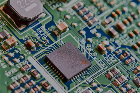
1. Surface Mount Technology (SMT)
Surface Mount Technology (SMT) is a PCB fabrication technique that involves mounting electronic components directly onto the surface of a PCB. SMT has become increasingly popular in recent years due to its ability to create smaller, more compact PCBs with higher component density.
Advantages of SMT
- Smaller PCB size
- Higher component density
- Faster assembly process
- Lower cost
Disadvantages of SMT
- Requires specialized equipment
- More difficult to repair than through-hole technology
- Requires more precise component placement

2. Through-Hole Technology
Through-hole technology is a PCB fabrication technique that involves drilling holes through the PCB and inserting electronic components into the holes. The components are then soldered onto the PCB to create a secure connection.
Advantages of Through-Hole Technology
- More reliable than SMT
- Easier to repair than SMT
- Better for high-power applications
Disadvantages of Through-Hole Technology
- Larger PCB size
- Lower component density
- Slower assembly process

3. Multi-Layer PCBs
Multi-layer PCBs are PCBs that contain more than two layers of conductive material. Multi-layer PCBs are used in applications that require high component density and complex circuit designs.
Advantages of Multi-Layer PCBs
- Higher component density
- More complex circuit designs
- Better signal integrity
- Reduced electromagnetic interference (EMI)
Disadvantages of Multi-Layer PCBs
- More expensive than single-layer PCBs
- More difficult to manufacture
- Requires specialized equipment

4. Flexible PCBs
Flexible PCBs are PCBs that are made from flexible materials such as polyimide or polyester. Flexible PCBs are used in applications that require the PCB to bend or flex, such as in wearable devices or medical equipment.
Advantages of Flexible PCBs
- Can bend and flex without breaking
- Lightweight and thin
- Can be used in tight spaces
Disadvantages of Flexible PCBs
- More expensive than rigid PCBs
- More difficult to manufacture
- Limited component options
5. High Density Interconnect (HDI) PCBs
High Density Interconnect (HDI) PCBs are PCBs that have a higher wiring density than traditional PCBs. HDI PCBs are used in applications that require high-speed data transfer and high component density.
Advantages of HDI PCBs
- Higher wiring density
- Faster data transfer speeds
- Smaller PCB size
- Lower power consumption
Disadvantages of HDI PCBs
- More expensive than traditional PCBs
- More difficult to manufacture
- Requires specialized equipment
6. Rigid-Flex PCBs
Rigid-flex PCBs are a combination of rigid and flexible PCBs. Rigid-flex PCBs are used in applications that require the PCB to have both rigid and flexible sections, such as in aerospace or military equipment.
Advantages of Rigid-Flex PCBs
- Combines the benefits of rigid and flexible PCBs
- Can be used in harsh environments
- Reduces the number of connectors required
Disadvantages of Rigid-Flex PCBs
- More expensive than traditional PCBs
- More difficult to manufacture
- Requires specialized equipment
7. Copper Thickness
Copper thickness refers to the thickness of the copper layer on a PCB. The thickness of the copper layer can affect the electrical properties of the PCB, such as its current-carrying capacity and impedance.
Standard Copper Thicknesses
| Copper Weight (oz) | Thickness (mm) |
|---|---|
| 0.5 | 0.017 |
| 1 | 0.035 |
| 2 | 0.070 |
| 3 | 0.105 |
Advantages of Thicker Copper
- Higher current-carrying capacity
- Better heat dissipation
- Improved signal integrity
Disadvantages of Thicker Copper
- More expensive
- More difficult to etch
- Can cause warping of the PCB
8. Solder Mask
Solder mask is a layer of protective coating that is applied to the surface of a PCB. The solder mask protects the copper traces on the PCB from oxidation and prevents solder bridges from forming during the soldering process.
Advantages of Solder Mask
- Protects the PCB from oxidation and corrosion
- Prevents solder bridges from forming
- Improves the appearance of the PCB
- Can be used to create text and graphics on the PCB
Disadvantages of Solder Mask
- Can affect the electrical properties of the PCB
- Can be difficult to remove for repairs
- Can be expensive for small batches
9. Silkscreen
Silkscreen is a layer of text and graphics that is printed onto the surface of a PCB. Silkscreen is used to label components, provide assembly instructions, and add branding to the PCB.
Advantages of Silkscreen
- Improves the readability of the PCB
- Provides assembly instructions
- Can be used for branding and marketing
- Can be used to create text and graphics on the PCB
Disadvantages of Silkscreen
- Can be expensive for small batches
- Can wear off over time
- Can be difficult to read on dark-colored PCBs
10. PCB Testing
PCB testing is an essential part of the PCB fabrication process. PCB testing ensures that the PCB is functioning correctly and meets the required specifications.
Types of PCB Testing
- Visual inspection
- Electrical testing
- Functional testing
- Environmental testing
- Burn-in testing
Advantages of PCB Testing
- Ensures the PCB is functioning correctly
- Identifies defects and errors early in the manufacturing process
- Reduces the risk of product failure in the field
- Improves customer satisfaction
Disadvantages of PCB Testing
- Can be time-consuming
- Can be expensive
- Requires specialized equipment and trained personnel
Frequently Asked Questions (FAQ)
1. What is the difference between SMT and through-hole technology?
SMT involves mounting components directly onto the surface of the PCB, while through-hole technology involves inserting components into holes drilled through the PCB and soldering them in place. SMT allows for smaller PCBs with higher component density, while through-hole technology is more reliable and easier to repair.
2. What are multi-layer PCBs used for?
Multi-layer PCBs are used in applications that require high component density and complex circuit designs. They offer better signal integrity and reduced electromagnetic interference compared to single-layer PCBs.
3. What are the advantages of flexible PCBs?
Flexible PCBs can bend and flex without breaking, making them ideal for use in wearable devices and medical equipment. They are also lightweight and thin, and can be used in tight spaces.
4. What is the purpose of solder mask on a PCB?
Solder mask is a protective coating that is applied to the surface of a PCB. It protects the copper traces from oxidation and prevents solder bridges from forming during the soldering process. Solder mask also improves the appearance of the PCB and can be used to create text and graphics.
5. Why is PCB testing important?
PCB testing is essential to ensure that the PCB is functioning correctly and meets the required specifications. It helps to identify defects and errors early in the manufacturing process, reducing the risk of product failure in the field and improving customer satisfaction.
Conclusion
PCB fabrication is a complex process that involves various techniques and processes. The 10 must-know PCB fabrication techniques discussed in this article are essential for creating high-quality PCBs that meet the required specifications. From SMT and through-hole technology to multi-layer and flexible PCBs, each technique has its own advantages and disadvantages. Copper thickness, solder mask, and silkscreen are also important considerations in PCB fabrication, as they can affect the electrical properties and appearance of the PCB. Finally, PCB testing is an essential part of the fabrication process, ensuring that the PCB is functioning correctly and meets the required specifications. By understanding these PCB fabrication techniques, designers and manufacturers can create high-quality PCBs that meet the needs of their customers.
No responses yet