What is PCB etching?
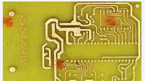
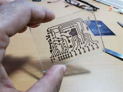
PCB etching is the process of removing unwanted copper from a printed circuit board (PCB) to create the desired circuit pattern. This is typically done using a chemical solution called an etchant, which selectively removes the copper while leaving the protected areas intact.
Disadvantage 1: Safety Concerns
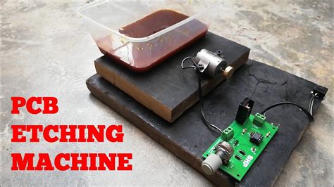
One of the primary disadvantages of PCB etching at home is the safety risks involved. The process requires the use of hazardous chemicals, such as ferric chloride or ammonium persulfate, which can cause serious harm if not handled properly.
| Chemical | Hazards |
|---|---|
| Ferric Chloride | – Corrosive to skin and eyes – Can cause respiratory irritation – Harmful if swallowed |
| Ammonium Persulfate | – Strong oxidizer – Can cause severe skin and eye irritation – May cause allergic respiratory reaction |
To minimize these risks, it’s essential to:
– Wear appropriate personal protective equipment (PPE) such as gloves, safety glasses, and a respirator
– Work in a well-ventilated area
– Follow proper handling and disposal procedures
Disadvantage 2: Environmental Impact
PCB etching chemicals can have a significant environmental impact if not disposed of properly. These chemicals can contaminate soil and water sources, harming wildlife and ecosystems.
To reduce the environmental impact of PCB etching, consider:
– Using less hazardous alternatives, such as citric acid or hydrogen peroxide
– Properly neutralizing and disposing of used etchant solutions
– Recycling or properly disposing of copper waste

Disadvantage 3: Time-Consuming Process
Etching PCBs at home can be a time-consuming process, especially for beginners. The steps involved, such as designing the circuit, transferring the pattern, and etching the board, can take several hours to complete.
| Step | Estimated Time |
|---|---|
| Circuit Design | 1-3 hours |
| Pattern Transfer | 30 minutes – 1 hour |
| Etching | 30 minutes – 2 hours |
| Cleaning and Finishing | 30 minutes – 1 hour |
To save time, consider:
– Using pre-sensitized PCB boards
– Investing in a high-quality laser printer for transferring patterns
– Using a temperature-controlled etching tank
Disadvantage 4: Limited Board Complexity
Home PCB etching setups may have limitations when it comes to creating complex circuit designs. Fine-pitch components, high-density layouts, and multi-layer boards can be challenging to etch accurately without professional equipment.
To work around these limitations, consider:
– Simplifying your circuit design
– Using larger component packages
– Splitting complex designs into multiple single-layer boards
Disadvantage 5: Quality Control Issues
Achieving consistent quality when etching PCBs at home can be difficult. Factors such as etchant concentration, temperature, and etching time can all affect the final result, leading to potential issues like over-etching, under-etching, or uneven etching.
To improve quality control, consider:
– Using a hydrometer to monitor etchant concentration
– Maintaining consistent temperature with a temperature-controlled etching tank
– Regularly agitating the solution during etching
– Inspecting boards closely after etching and making necessary adjustments
Disadvantage 6: Equipment and Material Costs
Setting up a home PCB etching workspace can be costly, especially if you’re starting from scratch. You’ll need to invest in various equipment and materials, such as:
- Etching tank
- Chemical-resistant containers
- Personal protective equipment (PPE)
- Copper clad boards
- Etchant chemicals
- Drilling and cutting tools
While some of these items can be found at relatively low costs, the expenses can add up quickly, especially if you plan on making multiple boards or experimenting with different techniques.
Disadvantage 7: Space Requirements
PCB etching at home requires dedicated workspace, as the process involves the use of hazardous chemicals and can be messy. You’ll need a well-ventilated area with access to running water and proper chemical storage.
Consider the following when setting up your workspace:
– Choose a location away from living areas and food preparation spaces
– Ensure adequate ventilation to remove fumes
– Provide easy access to a sink or water source for cleaning and disposal
– Designate storage space for chemicals, equipment, and materials
Disadvantage 8: Steep Learning Curve
For those new to PCB fabrication, the learning curve for etching boards at home can be steep. You’ll need to familiarize yourself with various concepts and techniques, such as:
- PCB design software
- Image transfer methods
- Etching process parameters
- Troubleshooting common issues
To make the learning process easier, consider:
– Starting with simple, single-sided designs
– Following tutorials and guides from experienced hobbyists
– Joining online communities and forums for advice and support
– Attending workshops or classes on PCB fabrication
Disadvantage 9: Limited Scalability
Home PCB etching setups are generally not suitable for large-scale production or commercial purposes. The process is manual and time-consuming, making it difficult to produce high volumes of boards consistently.
If you plan on scaling up your PCB fabrication, consider:
– Outsourcing production to professional PCB manufacturers
– Investing in automated equipment, such as CNC routers or pick-and-place machines
– Exploring alternative fabrication methods, such as PCB milling or 3D printing
Disadvantage 10: Troubleshooting and Rework
Even with careful planning and execution, issues can arise during the PCB etching process. Common problems include:
- Incomplete etching
- Overetching
- Uneven etching
- Damaged or lifted traces
Troubleshooting and reworking these issues can be frustrating and time-consuming, especially for beginners. To minimize the need for rework, consider:
– Double-checking your design before etching
– Carefully monitoring the etching process
– Using high-quality materials and equipment
– Practicing proper technique and following best practices
FAQ
1. Is PCB etching at home safe?
PCB etching at home can be safe if proper precautions are taken, such as wearing appropriate PPE, working in a well-ventilated area, and following proper handling and disposal procedures. However, the process does involve the use of hazardous chemicals, so it’s essential to understand the risks and take necessary safety measures.
2. What are some alternatives to ferric chloride for PCB etching?
Some alternatives to ferric chloride for PCB etching include:
– Ammonium persulfate
– Cupric chloride
– Hydrogen peroxide and hydrochloric acid (HCl)
– Citric acid and hydrogen peroxide
3. How long does it take to etch a PCB at home?
The time required to etch a PCB at home can vary depending on factors such as the size and complexity of the board, the etching method used, and the experience of the person doing the etching. On average, the entire process can take anywhere from 2 to 6 hours, including design, pattern transfer, etching, and cleaning.
4. Can I etch multi-layer PCBs at home?
Etching multi-layer PCBs at home can be challenging and requires specialized equipment and techniques. While it is possible, it is generally not recommended for beginners. It’s usually more practical to outsource the fabrication of multi-layer boards to professional PCB manufacturers.
5. What should I do with used PCB etching chemicals?
Used PCB etching chemicals should be properly neutralized and disposed of in accordance with local regulations. Do not pour them down the drain or dispose of them in regular trash. Contact your local waste management authority for guidance on proper disposal methods in your area.
Conclusion
PCB etching at home can be a rewarding and educational experience for electronics enthusiasts. However, it’s crucial to understand the disadvantages and challenges associated with the process before getting started. By considering factors such as safety, environmental impact, time investment, and equipment costs, you can make an informed decision about whether home PCB etching is right for you. With proper planning, preparation, and practice, you can overcome these disadvantages and successfully create your own custom PCBs at home.
No responses yet